2015 publications

All-Optical Nanometric Switch Based on the Directional Scattering of Semiconductor Nanoparticles
Abstract
A structure based on a dimer of silicon nanoparticles, presenting directional scattering in the visible range, was studied as a new design of an all-optical switch. The combination of spherical nanoparticles satisfying, at the same incident wavelength, the zero-backward and the minimum-forward scattering conditions can produce either a maximum or a minimum of the scattered field in the area between the nanoparticles. The modulation of the incident wavelength can be used as a switching parameter due to the sensitivity of these conditions to it. An optimization of the dimer setup, both in the distance between the nanoparticles and the incident wavelength, was numerically performed to obtain a maximum contrast. Also, near-field and far-field distributions of the electric field have been considered.

Plasmonic Optical Interferences for Phase-Monitored Nanoscale Sensing in Low-Loss Three-Dimensional Metamaterials
Abstract
We report a powerful and general concept for the design of three-dimensional metamaterials suitable for optically probed nanoscale sensing, combining the environmental sensitivity of localized surface plasmon resonances (LSPRs) and a low absorption of the probe light, even when the LSPRs are supported by lossy plasmonic elements. This concept is based on the tuning of the plasmon-induced Brewster conditions (angle of incidence and photon energy) of the material by suitable tailoring of its structure. This tuning is made possible by the interplay between LSPRs and optical interferences, i.e., the so-called plasmonic optical interferences. The plasmon-induced Brewster photon energy can be set outside the spectral range of the LSPR, thus in a spectral region of low optical absorption. Such “off-resonant” plasmon-induced Brewster conditions are examplified in a self-assembled lamellar three-dimensional metamaterial consisting of stacked polymer layers doped with gold nanoparticles alternating with undoped polymer layers. At the “off-resonant” plasmon-induced Brewster conditions, an abrupt jump of the ellipsometric phase angle Δ occurs in the photon energy space. In the spectral vicinity of this jump, Δ shows strong sensitivity to the spectral features of the LSPR, potentially allowing the detection of infinitesimal LSPR energy shifts (<10–5 eV) with a low absorptive loss of the probe light. The proposed concept has a wide outreach, as it can be applied regardless of the nature of the plasmonic element. It is appealing for the design of a broad variety of metamaterials (in terms of structure and composition) with multiple embedded sensing functionalities.
Optical performance of thin films produced by the pulsed laser deposition of SiAlON and Er targets
Abstract
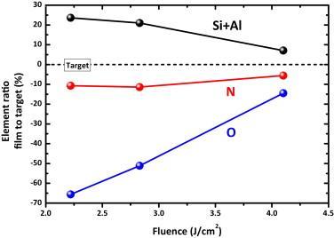
We report the preparation and optical performance of thin films produced by pulsed laser deposition in vacuum at room temperature, by focusing an ArF excimer laser onto two separate targets: a commercial ceramic SiAlON and a metallic Er target. As a result of the alternate deposition Er:SiAlON films were formed. The as grown films exhibited an Er-related emission peaking at 1532 nm. The role of the PLD energy density during deposition on the final matrix film was investigated, in order to achieve an optimized matrix composition with enhanced optical properties, and its effect on the light emission performance.

Importance of layer thermal conductivity on the sharpness of patterns produced by laser interference
Abstract
In this work, we compare patterns produced in Ag layers having similar thickness in the range 8.3–10.8 nm but having different initial nanostructure, i.e. behaving either as discontinuous or continuous layers and thus having very different thermal conductivities. The patterns are produced by exposing a phase mask to an excimer laser operating at 193 nm and using a projection optics that leads to similar fringed patterns with periods in the range 6.3–6.7 μm. The layer breaks up into isolated NPs due to laser induced melting at the regions around the intensity maxima sites. The resulting fringes have sharp interfaces in the case of discontinuous layers while a variety of regions across the pattern with no sharp interfaces are produced in the case of continuous layers. The results show that while the temperature distribution across the pattern matches almost perfectly the laser beam intensity profile for the former case, it becomes smeared due to lateral heat flow for the latter case. These results provide evidences for significant heating at the intensity minima sites that lead to solid-state dewetting and will eventually limit the minimum period achievable in the case of continuous metal layers or thermally conducting layers.

Tailored Fringed Platforms Produced by Laser Interference for Aligned Neural Cell Growth
Abstract
Ordering neural cells is of interest for the development of neural interfaces. The aim of this work is to demonstrate an easy‐to‐use, versatile, and cost/time effective laser‐based approach for producing platforms that promote oriented neural growth. We use laser interferometry to generate fringed channels with topography on partially reduced graphene oxide layers as a proof‐of‐concept substrate. We study cell adhesion, morphology, viability, and differentiation in cultures of embryonic neural progenitor cells on platforms with a 9.4 μm period. Results evidence that fringed platforms significantly promote neurite alignment (≈50% at 6 d), while preserving viability and neural differentiation.

Tuning the plasmonic response of bimetallic films by laser irradiation
Abstract
This work shows that surface treatment of multilayer Au and Ag thin films with single UV nanosecond laser pulses is a versatile and an easy-to-use tool for tuning their optical response or colour in a wide spectral range. As a laser parameter, we have varied the fluence. As film parameters, we have studied the film configuration by changing the deposition order, number of layers as well as the composition by varying the thickness of the Au layer while keeping that of Ag constant. The laser exposure produces melting of the layers followed by mixing of the two metals and dewetting, which lead to nanoparticle (NP) formation. The optical response is dominated by the surface plasmon resonance (SPR) associated to the NPs whose wavelength, intensity and bandwidth are consistent with the observed NP morphologies, the number density and the variation of optical constants with Au content. It is dominated by the balance between the interband transition onset of the alloy and the SPR of the nanoalloyed NPs for low fluences and by multipolar interactions for high fluences. While the Au content allows tuning the SPR in the range of ≈ 180 nm, the laser fluence allows a fine tuning of the SPR features and the film configuration has little impact on the optical response. All together this allows tuning the colour in ranges broader than 20 CIELAB units along the two chromatic axes.
3D laser-written silica glass step-index high-contrast waveguides for the 3.5 µm mid-infrared range
Abstract
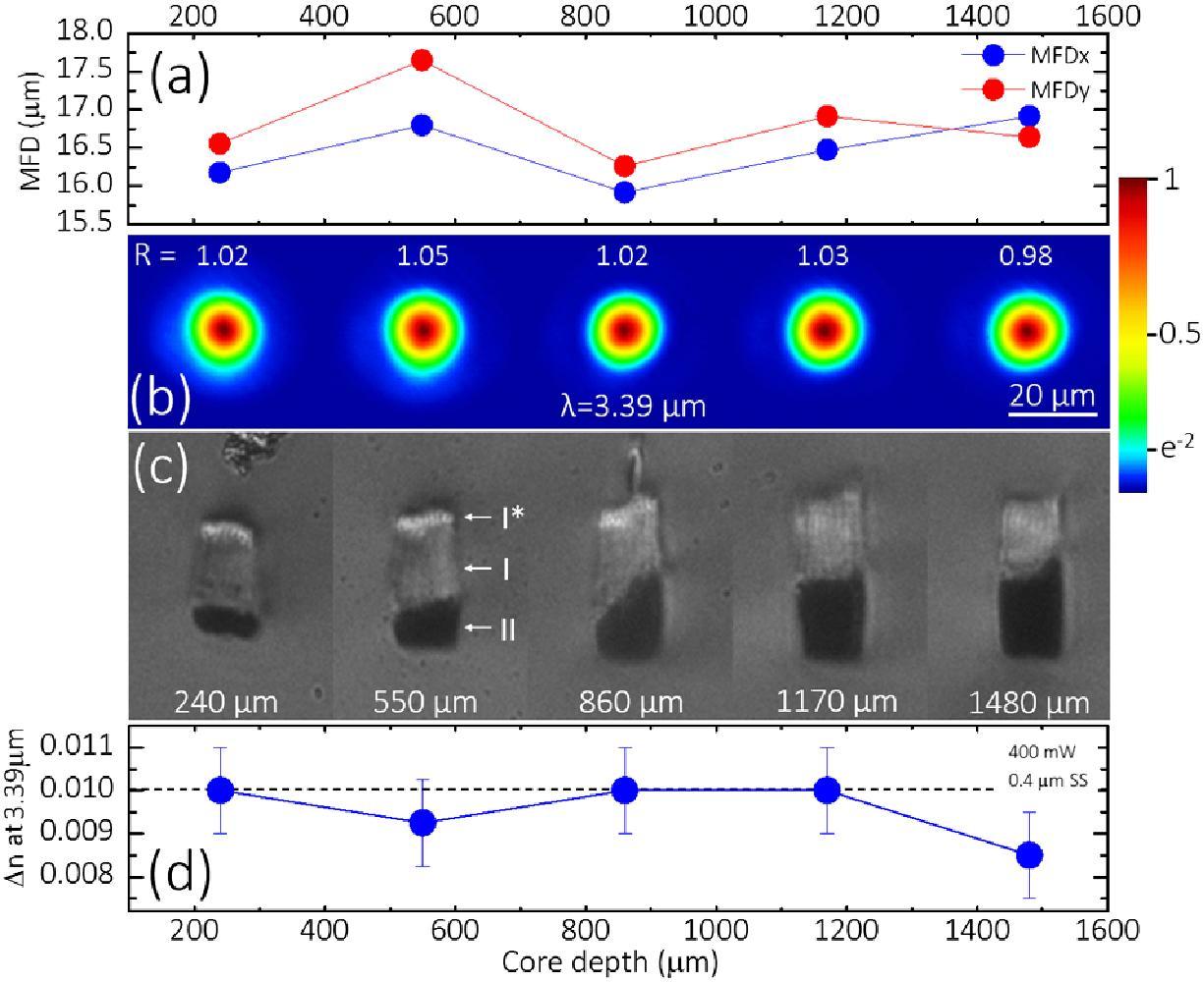
We report on the direct laser fabrication of step-index waveguides in fused silica substrates for operation in the 3.5 μm mid-infrared wavelength range. We demonstrate core-cladding index contrasts of 0.7% at 3.39 μm and propagation losses of 1.3 (6.5) dB/cm at 3.39 (3.68) μm, close to the intrinsic losses of the glass. We also report on the existence of three different laser modified SiO2 glass volumes, their different micro-Raman spectra, and their different temperature-dependent populations of color centers, tentatively clarifying the SiO2 lattice changes that are related to the large index changes.
© 2015 Optical Society of America

Femtosecond-laser induced compositional changes for high performance photonics applications
Abstract
Using femtosecond (fs) lasers to generate subsurface structures in transparent materials has led to a variety of applications. Among them, the production of photonic and microfluidic components has been particularly successful.1 Direct laser writing of subsurface structures2 is based on the use of an ultrafast laser beam that is focused underneath the surface. The multiphoton and impact ionization that occurs in the focal region as a result of this interaction leads to material modification: see Figure 1. Provided that a sufficiently large refractive index contrast (Δn) is induced in the transformed region, light-guiding elements with a 2D or 3D configuration can be fabricated using this technique.
Mirrorless KYW:Yb3+ waveguide laser combining liquid phase epitaxy and multiplexed beam fs laser writing
Abstract
In this paper, a mirrorless Yb 3+ -doped KY 1-x-y Gd x Lu y (WO 4 ) 2 waveguide laser with cw operation at 981.5 and 1001 nm, fabricated by liquid phase epitaxy and femtosecond laser microstructuring, is reported. A planar waveguide was fabricated by growing an Yb 3+ -doped KY 1-x-y Gd x Lu y (WO 4 ) 2 epitaxial layer by liquid phase epitaxy over a KY(WO 4 ) 2 substrate. This planar waveguide was then microstructured by means of a multiplexed beam femtosecond laser writing technique in order to define ridge waveguides. Mirrorless laser action is demonstrated in ridge waveguides with different fabrication parameters, obtaining maximum slope efficiency of 78% versus absorbed power, which confirms the feasibility of this technique for the development of integrated laser devices.
Growth of ZnO nanostructures by femtosecond laser irradiation of polycrystalline targets
Abstract
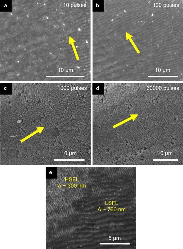
The formation of LIPSS upon irradiation with ultrashort laser pulses on the surface of polycrystalline ZnO samples and the potential use of irradiated areas as growth patterns for the production of highly ordered nanostructures upon redeposition have been studied. For this purpose, we have performed different sets of irradiation experiments including static irradiation experiments at low and high repetition rates, as well as scanned beam experiments at high repetition rate, this later in order to generate relatively large template regions for nanostructure growth by redeposition. In all cases, LIPSS formation has been achieved in the ZnO polycrystalline surface. Under appropriate irradiation conditions, the material is redeposited rendering a high density of nanostructures with high aspect ratios and good crystal quality. Given the special luminescent properties and applications of ZnO, particular attention has been paid to the luminescence properties after irradiation and after post-irradiation thermal treatments. The observed evolution has been correlated with evolution of point defects in the treated surfaces. Thermal treatments cause significant changes in both the topography and the cathodoluminescent emission, such as the development of laminar structures, the emergence of nucleation centers and the recovery of ultraviolet emission previously quenched as a consequence of irradiation. Interestingly, LIPSS remain after the luminescent recovery by thermal annealing, opening the possibility to control both luminescence properties and grain size while maintaining an ordered structure with a high effective surface area.
Channel waveguide fabrication technique in KY(WO4)2 combining liquid-phase-epitaxy and beam-multiplexed fs-laser writing
Abstract
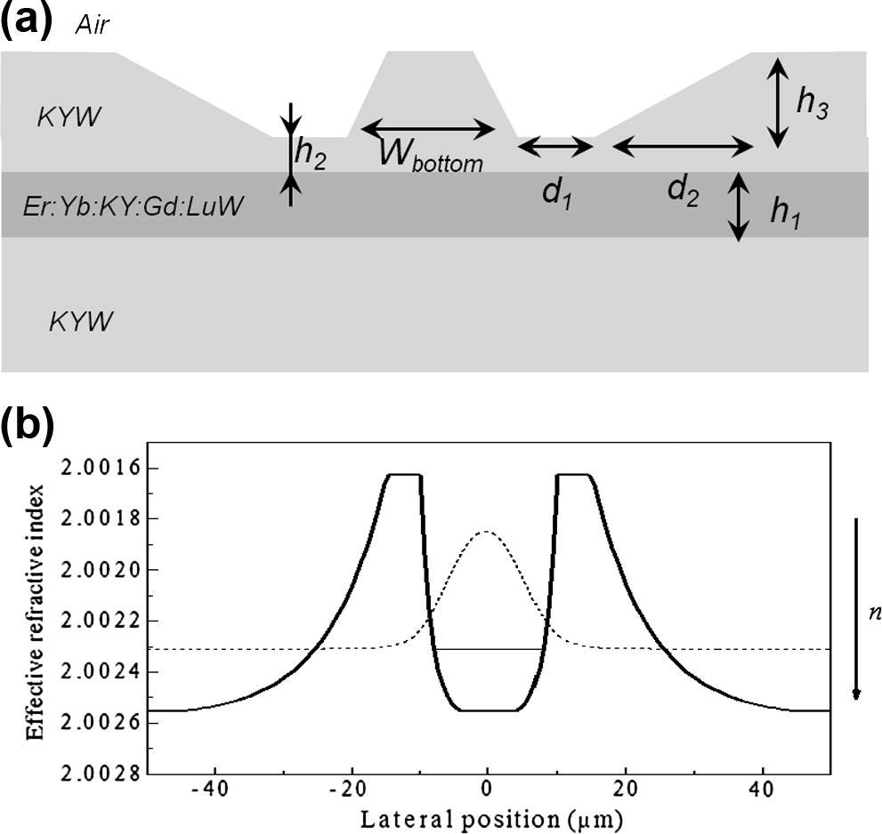
In the present work we propose a 2D-channel waveguide fabrication process based on the microstructuration of the cladding of a planar waveguide by femtosecond laser writing. The core of the waveguide is formed by a layer of KY1−x−yGdxLuy(WO4)2 epitaxially grown over a KY(WO4)2 substrate by means of Liquid Phase Epitaxy (LPE). A cladding of KY(WO4)2 is then grown by LPE over the core waveguide. To obtain lateral light confinement, the cladding is then micromachined using a multiplexed femtosecond laser writing beam, forming a ridge structure. Channel waveguides fabricated following this approach have been characterized in terms of their mode sizes and propagation losses at 0.98 μm and 1.64 μm, which are close to the wavelengths of interest in lasers/amplifiers based on the Er3+/Yb3+ system. Experimental data are compared with simulation analysis based on the Effective Index Method and the Beam Propagation Method, showing a good accordance between experimental and numerical results.

Rare earth-ion/nano-silicon ultrathin layer: A versatile nano-hybrid light-emitting building block for active optical metamaterials
Abstract
We fabricate an Er3+/nano-Si ultrathin (≈ 4 nm) layer and explore its optical response from the near-UV to the near-IR, in the linear and nonlinear regimes. This nanohybrid layer combines the tunable broad-band light harvesting properties of nano-Si with the robust and sharp Er3+ light emission. Its unique nanostructure enables efficient nanometer-range transfer of the harvested energy to the Er3+ ions. Therefore, clear 1.54 μm Er3+ photoluminescence (PL) is observed under excitation at any photon energy (Eexc) from the visible to the near-UV, despite the small amount of Er3+ ions in the layer (<2.5% of atomic monolayer). In the linear regime, the Er3+ PL intensity can be tuned to a maximum by setting the amount of nano-Si (QSi) in the layer at a suitable value, independent of Eexc. In the nonlinear regime, adjustment of QSi allows the dependence of the Er3+ PL intensity on Eexc to be tuned and achievement of nonconventional saturation properties not reported so far in Er3+:nano-Si systems. Based on this characteristic tunability, at sufficiently low QSi the nanohybrid layer is an ideal candidate for efficient near-IR emission under intense near UV–visible broad-band excitation. Furthermore, the nanohybrid layers with high enough QSi show an interesting potential for the optical modulation of the PL intensity by using UV light in a pump–probe configuration. Therefore, this nanohybrid layer is an outstanding candidate as a pure-color light-emitting building block for the development of advanced multiscale active optical metamaterials.

Controlling plasma distributions as driving forces for ion migration during fs laser writing
Abstract
The properties of structures written inside dielectrics with high repetition rate femtosecond lasers are known to depend strongly on the complex interplay of a large number of writing parameters. Recently, ion migration within the laser-excited volume has been identified as a powerful mechanism for changing the local element distribution and producing efficient optical waveguides. In this work it is shown that the transient plasma distribution induced during laser irradiation is a reliable monitor for predicting the final refractive index distribution of the waveguide caused by ion migration. By performing in situ plasma emission microscopy during the writing process inside a La-phosphate glass it is found that the long axis of the plasma distribution determines the axis of ion migration, being responsible for the local refractive index increase. This observation is also valid when strong positive or negative spherical aberration is induced, greatly deforming the focal volume and inverting the index profile. Even subtle changes in the writing conditions, such as an inversion of the writing direction (quill writing effect), show up in the form of a modified plasma distribution, which manifests as a modified index distribution. Finally, it is shown that the superior control over the waveguide properties employing the slit shaping technique is caused by the more confined plasma distribution produced. The underlying reasons for this unexpected result are discussed in terms of non-linear propagation and heat accumulation.
Nanofabrication of Tailored Surface Structures in Dielectrics Using Temporally Shaped Femtosecond-Laser Pulses
Abstract
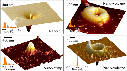
We have investigated the use of tightly focused, temporally shaped femtosecond (fs)-laser pulses for producing nanostructures in two dielectric materials (sapphire and phosphate glass) with different characteristics in their response to pulsed laser radiation. For this purpose, laser pulses shaped by third-order dispersion (TOD) were used to generate temporally asymmetric excitation pulses, leading to the single-step production of subwavelength ablative and subablative surface structures. When compared to previous works on the interaction of tightly focused TOD-shaped pulses with fused silica, we show here that this approach leads to very different nanostructure morphologies, namely, clean nanopits without debris surrounding the crater in sapphire and well-outlined nanobumps and nanovolcanoes in phosphate glass. Although in sapphire the debris-free processing is associated with the much lower viscosity of the melt compared to fused silica, nanobump formation in phosphate glass is caused by material network expansion (swelling) upon resolidification below the ablation threshold. The formation of nanovolcanoes is a consequence of the combined effect of material network expansion and ablation occurring in the periphery and central part of the irradiated region, respectively. It is shown that the induced morphologies can be efficiently controlled by modulating the TOD coefficient of the temporally shaped pulses.

Rapid assessment of nonlinear optical propagation effects in dielectrics
Abstract
Ultrafast laser processing applications need fast approaches to assess the nonlinear propagation of the laser beam in order to predict the optimal range of processing parameters in a wide variety of cases. We develop here a method based on the simple monitoring of the nonlinear beam shaping against numerical prediction. The numerical code solves the nonlinear Schrödinger equation with nonlinear absorption under simplified conditions by employing a state-of-the art computationally efficient approach. By comparing with experimental results we can rapidly estimate the nonlinear refractive index and nonlinear absorption coefficients of the material. The validity of this approach has been tested in a variety of experiments where nonlinearities play a key role, like spatial soliton shaping or fs-laser waveguide writing. The approach provides excellent results for propagated power densities for which free carrier generation effects can be neglected. Above such a threshold, the peculiarities of the nonlinear propagation of elliptical beams enable acquiring an instantaneous picture of the deposition of energy inside the material realistic enough to estimate the effective nonlinear refractive index and nonlinear absorption coefficients that can be used for predicting the spatial distribution of energy deposition inside the material and controlling the beam in the writing process.

Controlling ablation mechanisms in sapphire by tuning the temporal shape of femtosecond laser pulses
Abstract
We have analyzed the influence of the temporal pulse shape on femtosecond (fs) laser-induced surface ablation processes in sapphire. To this end, single transform-limited (TL), stretched, and third-order-dispersion (TOD) shaped fs pulses have been used, while the dynamics of the interaction were analyzed by fs-resolved microscopy and correlated with plasma emission intensity and crater morphology. The modification of the pulse shape enables changing the ablation mechanism from a strong, thermally mediated ablation process to a gentle ablation process mediated by Coulomb explosion (CE), with respective ablation depths of 100–200 nm and 5–10 nm. Analysis of the transient optical response allows direct comparison of the transient plasma carrier densities involved, observing comparable peak values for both processes. For strong ablation induced by TL pulses, a direct relation between plasma density and local ablation depth is found, but this does not hold for the CE-mediated process observed for TOD-shaped pulses. For TOD-shaped pulses at very high fluence, a different ablation mechanism involving explosive boiling is identified. This mechanism leads to the formation of deep craters with reduced lateral extension and steep walls. This amount of control over the ablation mechanisms by a simple selection of the pulse shape should be of interest for new surface structuring approaches.
© 2014 Optical Society of America

Dual Regimes of Ion Migration in High Repetition Rate Femtosecond Laser Inscribed Waveguides
Abstract
Ion migration in high repetition rate femtosecond laser inscribed waveguides is currently being reported in different optical glasses. For the first time, we discuss and experimentally demonstrate the presence of two regimes of ion migration found in laser written waveguides. Regime-I corresponds to the initial waveguide formation mainly via light element migration (in our case atomic weight <; 31 u), whereas regime-II majorly corresponds to the movement of heavy elements. This behavior brings attention to a problem which has never been analyzed before and that affects the laser written active waveguides, in which active ions migrate changing their local spectroscopic properties. The migration of active ions may in fact detune the predesigned optimal values of active photonic devices. This letter experimentally demonstrate this problem and provides solutions to avert it.

Laser Treatment of Ag@ZnO Nanorods as Long Lifespan SERS Surfaces
Abstract
UV nanosecond laser pulses have been used to produce a unique surface nanostructuration of Ag@ZnO supported nanorods (NRs). The NRs were fabricated by plasma enhanced chemical vapor deposition (PECVD) at low temperature applying a silver layer as promoter. The irradiation of these structures with single nanosecond pulses of an ArF laser produces the melting and reshaping of the end of the NRs that aggregate in the form of bundles terminated by melted ZnO spherical particles. Well-defined silver nanoparticles (NPs), formed by phase separation at the surface of these melted ZnO particles, give rise to a broad plasmonic response consistent with their anisotropic shape. Surface enhanced Raman scattering (SERS) in the as-prepared Ag@ZnO NRs arrays was proved by using a Rhodamine 6G (Rh6G) chromophore as standard analyte. The surface modifications induced by laser treatment improve the stability of this system as SERS substrate while preserving its activity.

Dynamics of laser induced metal nanoparticle and pattern formation
Appl. Phys. Lett. 106, 061914 (2015)
Abstract
Discontinuous metal films are converted into either almost round, isolated, and randomly distributed nanoparticles (NPs) or fringed patterns of alternate non transformed film and NPs by exposure to single pulses (20 ns pulse duration and 193 nm wavelength) of homogeneous or modulated laser beam intensity. The dynamics of NPs and pattern formation is studied by measuring in real time the transmission and reflectivity of the sample upon homogeneous beam exposure and the intensity of the diffraction orders 0 and 1 in transmission configuration upon modulated beam exposure. The results show that laser irradiation induces melting of the metal either completely or at regions around intensity maxima sites for homogeneous and modulated beam exposure, respectively, within ≤10 ns. The aggregation and/or coalescence of the initially irregular metal nanostructures is triggered upon melting and continues after solidification (estimated to occur at ≤80 ns) for more than 1 μs. The present results demonstrate that real time transmission rather than reflectivity measurements is a valuable and easy-to-use tool for following the dynamics of NPs and pattern formation. They provide insights on the heat-driven processes occurring both in liquid and solid phases and allow controlling in-situ the process through the fluence. They also evidence that there is negligible lateral heat release in discontinuous films upon laser irradiation.
R.J.P., T.K., and C.E.R., respectively, acknowledge the Grant No. JCI-2012_13034 from the Juan de la Cierva program, the support of DAAD, and CONACYT-México postdoctoral fellowship No. 175641. The authors gratefully thank Professor P. Leiderer from University of Konstanz for his support and the Electron Microscopy Laboratory of CENIM for helping with the SEM observations.

Density patterns in metal films produced by laser interference
Abstract
Fringed periodic patterns have been produced by laser interference at 193 nm in an almost continuous 9.5 nm-thick Ag film that exhibits a number density of ≈189 μm−2 holes. Patterns with four periods in the range of 1.8–10.2 μm were produced by changing the projection optics. At high fluences, the film breaks up into nanostructures around the regions exposed to intensity maxima due to laser-induced melting. At low fluences, a new process is observed that is triggered at the initial holes of the film by solid-state dewetting. Once the fluence is high enough to prevent the temperature balance across the pattern, mass transport from cold to hot regions is observed, leading to film densification in regions around intensity maxima sites. The novel patterns are thus formed by fringes of material that is more/less dense than the as-grown film, each of which is located at intensity maxima/minima sites, and have negligible topography. Comparing the present results to earlier reports in the literature shows that the thermal gradient across the pattern is influenced by the initial film microstructure, rather than by the thickness. The existence of a minimum period, which is achievable depending on the thermal continuity of the film, is also discussed.

Thermo-optical properties of Bi nanoparticles embedded in germanate glasses and alumina thin films
Abstract
Materials, and particularly glasses, with a tailor-made spectral optical response that can be switched in a controlled way using external stimuli excitation are of interest for the development of active optical devices, such as active filters or all-optical switching components. Based on the dielectric functions of solid and liquid bismuth (Bi), it is expected that both solid and liquid Bi nanostructures will show optical resonances with relevant different features in the near ultraviolet to near infrared. In addition, Bi has a low melting point that enables the solid–liquid phase change under moderate heating. Profiting of these singular properties we present and review in this paper the main results that have been obtained in our laboratory concerning the thermo-optical response of bulk germanate glasses and amorphous Al2O3 thin films with embedded Bi nanoparticles (NPs). In both materials the optical transmission as a function of the temperature shows broad hysteresis loops. The optical contrast and width of these cycles depend on the Bi content and NP size. From the successful modelling of the optical properties of the Bi NPs-doped glasses, it is proposed that the observed material thermo-optical response arises from the change in the dielectric function of the Bi NPs upon melting, which induces relevant changes in the resonant optical behaviour of the Bi NPs. These results suggest that glasses with embedded Bi NPs are promising for the design of spectral-selective thermo-optical devices.

Period dependence of laser induced patterns in metal films
Abstract
Periodic fringed patterns with four periods in the range 1.8–10.2 μm have been produced in continuous Ag films that have thicknesses of 14.6 nm and 19.5 nm by exposing a phase mask to single pulses of an excimer laser operating at 193 nm. The films were patterned either as-grown or after homogeneous exposure to the same laser beam. For fluences above the threshold, the films undergo liquid-state dewetting that, from low to high fluences, leads to their break into holes, fingers or elongated features and finally to isolated nanoparticles irrespective of the period, thickness or fluence. The period determines the range of fluences to achieve the different morphologies since the temperature profile across the pattern depends on the period due to the existence of significant lateral heat flow across the pattern. The maximum temperature achieved at the intensity maxima/minima sites thus decreases/increases as the period decreases, leading to solid-state dewetting at regions around the intensity minima; the shorter the period, the higher this type of dewetting. These regions eventually overcome the melting temperature for the shortest period and intermediate fluence, leading to the complete transformation of the films. Finally, the initial film morphology (discontinuities or holes) rather than thickness plays an essential role in the level of transformation at fluences around the threshold.

