2020 Publications
Waveguide tapers fabrication by femtosecond laser induced element redistribution in glass
Manuel Macias-Montero, Antonio Dias, Belen Sotillo, Pedro Moreno-Zarate, Rocio Ariza, Paloma Fernandez, Javier Solis
Journal of Lightwave Technology (2020).
Abstract
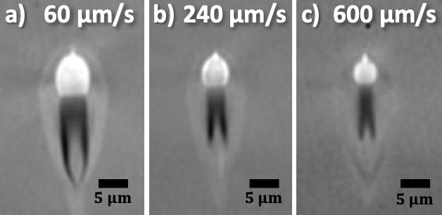
Here in we present the fabrication and performance of waveguide tapers produced by femtosecond laser induced element redistribution in modified phosphate glasses. More particularly, it is demonstrated that by controlling the scan velocity during the writing process it is possible to adequately tune both the size of the modified area and the refractive index contrast to produce waveguides that can cope with mode filed diameters in the range of 7-16 μm. In addition, we fabricated tapered structures through the induction of an acceleration in the laser scanning velocity, resulting in a device that can efficiently convert a wide range of mode fields. The fine control achieved over the index contrast in the range of 10−3 and 10−2 would allow the production of a wide variety of tapers that could potentially be used to couple numerous photonic devices.
Self‐Assembled, 10 nm‐Tailored, Near Infrared Plasmonic Metasurface Acting as Broadband Omnidirectional Polarizing Mirror
Esther Soria, Pilar Gomez‐Rodriguez, Christophe Tromas, Sophie Camelio, David Babonneau, Rosalia Serna, José Gonzalo, Johann Toudert
Advanced Optical Materials, 2000231 (2020).
Abstract
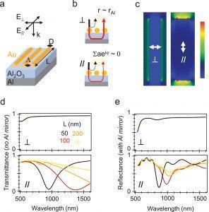
Plasmonic metasurfaces tailored at the few‐nanometers scale and fabricated by high‐throughput lithography‐free methods are needed to efficiently produce optical components with optimal performance and small footprint. Herein, the design of such metasurfaces and their fabrication over cm2 areas by self‐assembly are reported. They present an optical cavity structure, in which a 2D array of parallel Au nanorods is coupled to a metal mirror through a thin spacer. The nanorods present a quasi‐monodisperse ≈10 nm diameter and separation, and a broad polydisperse length distribution. These remarkable nanostructural features, combining periodicity in one direction with randomness in another, endow the nanorod array with unconventional plasmonic and anisotropic effective optical properties. Thanks to these properties, for light polarized along the nanorods, the metasurface displays strong destructive optical interference and thus near‐perfect absorption over a broad range of angles of incidence and of wavelengths in the near infrared. In contrast, for light polarized perpendicular to the nanorods, no such interference occurs and thus the metasurface behaves as a metal mirror. In sum, the metasurface can be used as broadband omnidirectional polarizing mirror, an original thin and monolithic optical component merging the functionalities of a metal mirror and of a wire‐grid polarizer.
Photoluminescence and Stoichiometry Correlation in Nanocrystalline EuOx Thin Films: Tunable Color Emission
A. Mariscal-Jiménez, A. Tarazaga Martín-Luengo, B. Galiana, C. Ballesteros, A. Bonanni, J. Martín-Sánchez, R. Serna
J. Phys. Chem. C, 124, 15434–15439, (2020)
Abstract
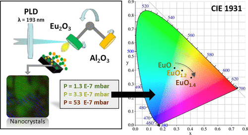
The development of broadband and ultracompact optoelectronic devices relies on the possibility of fabricating bright and tunable emitters at the nanoscale. Here, we show emission from EuOx (1 ≤ x < 1.4) thin films on silicon formed by nanocrystals with average sizes in the range of 5 nm. The photoluminescence emission of the nano-EuOx films is tunable as a function of the oxygen concentration changing from a green broadband Eu2+-related emission to a narrow red Eu3+-related emission. To reach these results has been instrumental through the use of a new methodology specially designed to achieve high-quality europium oxide films whose compositional properties are controlled by the growth base pressure and preserved thanks to a chemically stable and transparent cover layer of Al2O3. Our findings confirm the outstanding potential of nanostructured EuOx films as “one-compound” optical elements with tunable emission properties for their implementation in integrated silicon-based devices.
Generation, control and erasure of dual LIPSS in germanium with fs and ns laser pulses
Noemi Casquero, Yasser Fuentes-Edfuf, Raul Zazo, Javier Solis, Jan Siegel
J. Phys. D: Appl. Phys. 53, 485106 (2020)
Abstract
Laser-induced periodic surface structures (LIPSS) can readily be fabricated in virtually all types of materials and benefit from an efficient parallel patterning strategy that exploits self-organization. The wide range of different LIPSS types with different spatial scales and symmetries is continuously growing, addressing numerous of applications. Here, we report on the formation of two fundamentally different types of LIPSS on germanium upon exposure to femtosecond laser pulses (λ=800 nm, 130 fs), featuring different periods and orthogonal orientations. On the one hand, the well-known low-spatial frequency LIPSS (LSFL) with a period ≈λ and perpendicular orientation to the laser polarization are formed, which can be extended homogeneously in 2D by sample scanning. Additionally, extremely smooth ripples with a period ≈λ /2 and parallel orientation were generated at lower pulse numbers. We show that this new kind of ripples, named HSFL-∥, can be superimposed onto LSFL by increasing the pulse number, forming complex dual LIPSS with nanohill-like morphology. While exposure to multiple nanosecond laser pulses is found to trigger also the formation of LSFL, HSFL-∥ cannot be formed under these conditions, which points out the role of ultrafast excitation in the formation of the latter. By performing time-resolved reflectivity measurements, we are able to resolve the melting and solidification dynamics, revealing melting of a very shallow surface layer (< 20 nm) and melt durations of a few ns for both pulse durations pulses at the fluences employed for LIPSS formation. Finally, we demonstrate erasure of both types of LIPSS by exposure to single nanosecond pulses at high fluences, which paves the way for erasable multi-level data storage.
Optical-based thickness measurement of MoO3 nanosheets
S. Puebla, A. Mariscal-Jiménez, R. Serna, C. Munuera, and A. Castellanos-Gomez
Nanomaterials, 10, 1–10 (2020)
Abstract
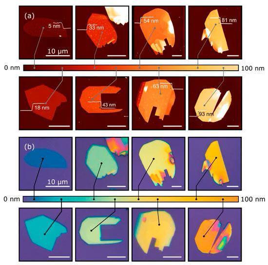
Considering that two-dimensional (2D) molybdenum trioxide has acquired more attention in the last few years, it is relevant to speed up thickness identification of this material. We provide two fast and non-destructive methods to evaluate the thickness of MoO3 flakes on SiO2/Si substrates. First, by means of quantitative analysis of the apparent color of the flakes in optical microscopy images, one can make a first approximation of the thickness with an uncertainty of ±3 nm. The second method is based on the fit of optical contrast spectra, acquired with micro-reflectance measurements, to a Fresnel law-based model that provides an accurate measurement of the flake thickness with ±2 nm of uncertainty.
On the properties of GaP supersaturated with Ti
J. Olea, S. Algaidy, A. del Prado, E. García-Hemme, R. Garcia-Hernansanz, D. Montero, D. Caudevilla, G. González-Diaz, E. Soria, J. Gonzalo.
Journal of Alloys and Compounds 820, 153358 (2020).
Abstract
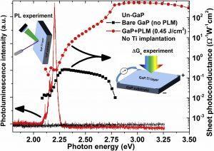
We have fabricated GaP supersaturated with Ti by means of ion implantation and pulsed-laser melting to obtain an intermediate band material with applications in photovoltaics. This material has a strong sheet photoconductance at energies below the bandgap of GaP and it seems to be passivated by a Ga defective GaPO oxide layer during the laser process. Passivation is consistently analyzed by sheet photoconductance and photoluminescence measurements. We report on the structural quality of the resulting layers and analyze the energy of the new optical transitions measured on GaP:Ti. A collapse found in the sheet photoconductance spectra of GaP:Ti samples fabricated on undoped substrates is explained by the negative photoconductivity phenomenon.
Deep UV laser induced periodic surface structures on silicon formed by self organization of nanoparticles
Raul Zazo, Javier Solis, José A. Sanchez-Gil, Rocio Ariza, Rosalía Serna and Jan Siegel
Applied Surface Science 520, 146307 (2020)
Abstract
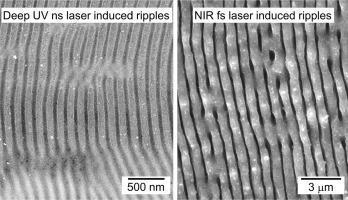
We have investigated the formation of laser-induced periodic surface structures (LIPSS or “ripples”) on silicon upon excitation with p-polarized excimer laser pulses in the deep ultraviolet region (λ = 193 nm, 20 ns). Well-pronounced ripples with a period close to the laser wavelength were observed for pulse numbers N ≥ 100, and the ripple period increased with the angle of incidence. While these results seem to be qualitatively consistent with the standard Sipe-theory, we observed a fundamentally different ripple formation mechanism and ripple morphology. At low pulse numbers, isolated nanoparticles with a size of a few tens of nanometers are observed at the silicon surface, which then start to agglomerate in 2D and self-organize to form ripples with a very shallow modulation depth as the pulse number increases. Employing a recently developed plasmonic model based on the propagation of a surface plasmon polariton on a rough surface, we demonstrate excellent quantitative agreement of the evolution of the ripple period with incidence angle. Finally, we show that surface regions exposed to lower laser fluence feature micro- and nanopores, which give rise to pronounced photoluminescence (PL) emission in the visible spectral region, as opposed to the nanoparticle-based ripples not showing PL.
Active analog tuning of the phase of light in the visible regime by bismuth-based metamaterials
Marina Garcia-Pardo, Eva Nieto-Pinero, Amanda K. Petford-Long, Rosalía Serna and Johann Toudert
Nanophotonics, 9, 885-896 (2020)
Abstract
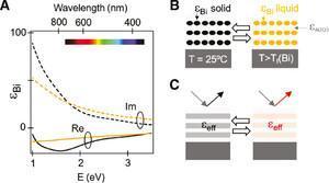
The active and analog tuning of the phase of light by metamaterials is needed to boost the switching performance of photonic devices. However, demonstrations of this type of tuning in the pivotal visible spectral region are still scarce. Herein, we report the active analog tuning of the phase of visible light reflected by a bismuth (Bi)-based metamaterial, enabled by a reversible solid-liquid transition. This metamaterial, fabricated by following a lithography-free approach, consists of two-dimensional assemblies of polydisperse plasmonic Bi nanostructures embedded in a refractory and transparent aluminum oxide matrix. The analog tuning of the phase is achieved by the controlled heating of the metamaterial to melt a fraction of the nanostructures. A maximum tuning of 320° (1.8 π) is observed upon the complete melting of the nanostructures at 230°C. This tuning is reversible by cooling to 25°C. In addition, it presents a wide hysteretic character due to liquid Bi undercooling. This enables the phase achieved by this analog approach to remain stable over a broad temperature range upon cooling and until re-solidification occurs around 100°C. Therefore, Bi-based metamaterials are endowed with analog optical memory capabilities, which are appealing for a wide range of applications, including optical data storage with enhanced information density or bistable photonic switching with a tunable “on” state.
Role of the La/K Compositional Ratio in the Properties of Waveguides Written by Fs-Laser Induced Element Redistribution in Phosphate-Based Glasses.
P. Moreno-Zarate, F. Muñoz, B. Sotillo, M. Macias-Montero, J. Atienzar, M. Garcia-Pardo, P. Fernandez, R. Serna, and J. Solis
Materials 13, 1275 (2020)
Abstract
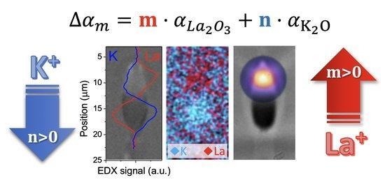
The local modification of the composition of glasses by high repetition femtosecond laser irradiation is an attractive method for producing photonic devices. Recently, the successful production of waveguides with a refractive index contrast (Δn) above 10−2 by fs-laser writing has been demonstrated in phosphate glasses containing La2O3 and K2O modifiers. This large index contrast has been related to a local enrichment in lanthanum in the light guiding region accompanied by a depletion in potassium. In this work, we have studied the influence of the initial glass composition on the performance of waveguides that are produced by fs-laser induced element redistribution (FLIER) in phosphate-based samples with different La and K concentrations. We have analyzed the contribution to the electronic polarizability of the different glass constituents based on refractive index measurements of the untreated samples, and used it to estimate the expected index contrast caused by the experimentally measured local compositional changes in laser written guiding structures. These estimated values have been compared to experimental ones that are derived from near field images of the guided modes with an excellent agreement. Therefore, we have developed a method to estimate before-hand the expected index contrast in fs-laser written waveguides via FLIER for a given glass composition. The obtained results stress the importance of considering the contribution to the polarizability of all the moving species when computing the expected refractive index changes that are caused by FLIER processes

Preferential Growth of ZnO Micro- and Nanostructure Assemblies on Fs-Laser-Induced Periodic Structures
B. Sotillo, R. Ariza, J. Siegel, J. Solis, and P. Fernández
Nanomaterials 10, 731 (2020).
Abstract
In this work, we demonstrate the use of laser-induced periodic surface structures (LIPSS) as templates for the selective growth of ordered micro- and nanostructures of ZnO. Different types of LIPSS were first produced in Si-(100) substrates including ablative low-frequency spatial (LSF) LIPSS, amorphous-crystalline (a–c) LIPSS, and black silicon structures. These laser-structured substrates were subsequently used for depositing ZnO using the vapor–solid (VS) method in order to analyze the formation of organized ZnO structures. We used scanning electron microscopy and micro-Raman spectroscopy to assess the morphological and structural characteristics of the ZnO micro/nano-assemblies obtained and to identify the characteristics of the laser-structured substrates inducing the preferential deposition of ZnO. The formation of aligned assemblies of micro- and nanocrystals of ZnO was successfully achieved on LSF-LIPSS and a–c LIPSS. These results point toward a feasible route for generating well aligned assemblies of semiconductor micro- and nanostructures of good quality by the VS method on substrates, where the effect of lattice mismatch is reduced by laser-induced local disorder and likely by a small increase of surface roughness
The Role of the Laser-Induced Oxide Layer in the Formation of Laser-Induced Periodic Surface Structures
C. Florian, J.-L. Déziel, S. V. Kirner, J. Siegel, and J. Bonse
Nanomaterials 10, 147 (2020).
Abstract
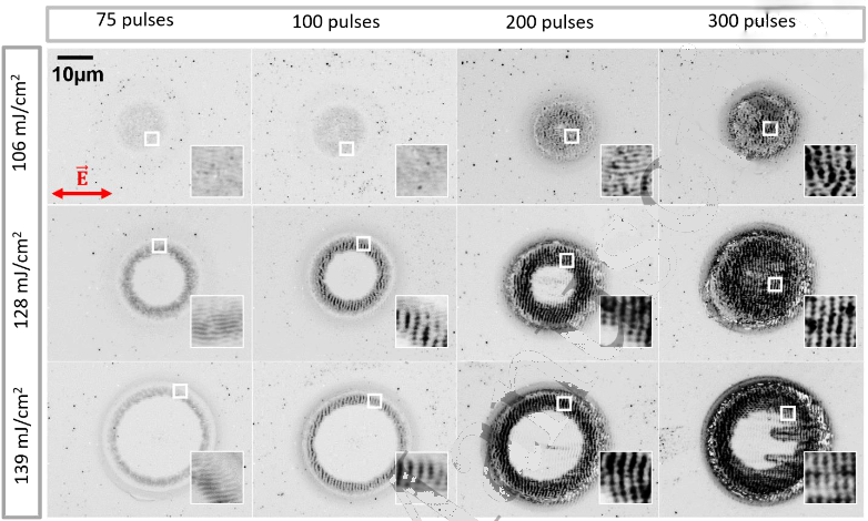
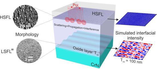
Laser-induced periodic surface structures (LIPSS) are often present when processing solid targets with linearly polarized ultrashort laser pulses. The different irradiation parameters to produce them on metals, semiconductors and dielectrics have been studied extensively, identifying suitable regimes to tailor its properties for applications in the fields of optics, medicine, fluidics and tribology, to name a few. One important parameter widely present when exposing the samples to the high intensities provided by these laser pulses in air environment, that generally is not considered, is the formation of a superficial laser-induced oxide layer. In this paper, we fabricate LIPSS on a layer of the oxidation prone hard-coating material chromium nitride in order to investigate the impact of the laser-induced oxide layer on its formation. A variety of complementary surface analytic techniques were employed, revealing morphological, chemical and structural characteristics of well-known high-spatial frequency LIPSS (HSFL) together with a new type of low-spatial frequency LIPSS (LSFL) with an anomalous orientation parallel to the laser polarization. Based on this input, we performed finite-difference time-domain calculations considering a layered system resembling the geometry of the HSFL along with the presence of a laser-induced oxide layer. The simulations support a scenario that the new type of LSFL is formed at the interface between the laser-induced oxide layer and the non-altered material underneath. These findings suggest that LSFL structures parallel to the polarization can be easily induced in materials that are prone to oxidation.
Spectroscopic ellipsometry study of Cu2ZnSn(SxSe1-x)4 bulk polycrystals
S. Levcenko, E. Hajdeu-Chicarosh, R. Serna, M. Guc, I. A. Victorov, A. Nateprov, I. V. Bodnar, R. Caballero, J. M. Merino, E. Arushanov, M. León.
J. Alloys Compd. 843, 1–6 (2020)
Abstract
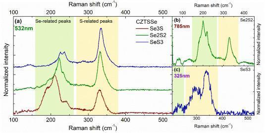
The pseudo dielectric function of Cu2ZnSn(SxSe1-x)4 [x = 0.35, 0.62, 0.81] bulk polycrystals is determined over the range 1.1–4.6 eV at room temperature from the analysis of spectroscopic ellipsometry data using the Adachi model. From the analysis, the lowest E0 transition and high energy E1A and E1B transitions are clearly identified, and used to follow the evolution of the pseudo dielectric function as a function of the composition. It is shown that the fundamental E0 and high energy E1A transitions can be tuned by increasing the sulfur content over a range of 0.3 eV. These results show the potential of the kesterite compounds for the design of efficient tailored photovoltaic solar cells.
Laser engineering of biomimetic surfaces
E Stratakis, Jörn Bonse, J Heitz, J Siegel, GD Tsibidis, E Skoulas, A Papadopoulos, A Mimidis, A-C Joel, P Comanns, Jörg Krüger, C Florian, Y Fuentes-Edfuf, J Solis, W Baumgartner
Materials Science and Engineering: R: Reports, 141, 100562 (2020)
Abstract
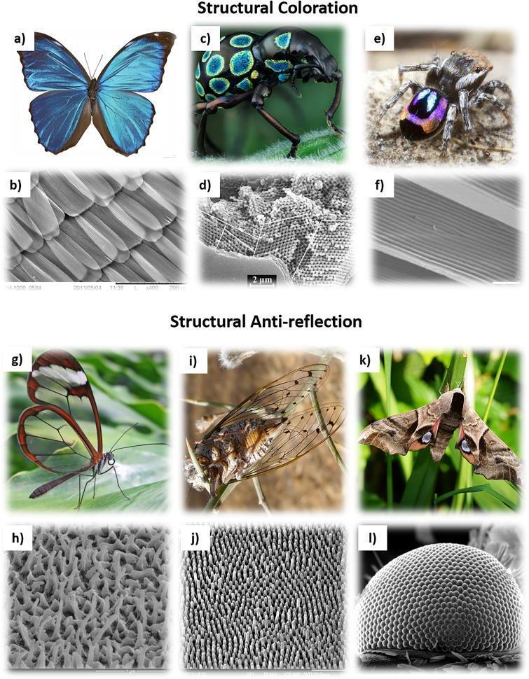
The exciting properties of micro- and nano-patterned surfaces found in natural species hide a virtually endless potential of technological ideas, opening new opportunities for innovation and exploitation in materials science and engineering. Due to the diversity of biomimetic surface functionalities, inspirations from natural surfaces are interesting for a broad range of applications in engineering, including phenomena of adhesion, friction, wear, lubrication, wetting phenomena, self-cleaning, antifouling, antibacterial phenomena, thermoregulation and optics. Lasers are increasingly proving to be promising tools for the precise and controlled structuring of materials at micro- and nano-scales. When ultrashort-pulsed lasers are used, the optimal interplay between laser and material parameters enables structuring down to the nanometer scale. Besides this, a unique aspect of laser processing technology is the possibility for material modifications at multiple (hierarchical) length scales, leading to the complex biomimetic micro- and nano-scale patterns, while adding a new dimension to structure optimization. This article reviews the current state of the art of laser processing methodologies, which are being used for the fabrication of bioinspired artificial surfaces to realize extraordinary wetting, optical, mechanical, and biological-active properties for numerous applications. The innovative aspect of laser functionalized biomimetic surfaces for a wide variety of current and future applications is particularly demonstrated and discussed. The article concludes with illustrating the wealth of arising possibilities and the number of new laser micro/nano fabrication approaches for obtaining complex high-resolution features, which prescribe a future where control of structures and subsequent functionalities are beyond our current imagination.


