Grupo de Procesado por Láser del Instituto de Óptica “Daza de Valdés”

Optical properties of differing nanolayered structures of divalent europium doped barium fluoride thin films synthesized by pulsed laser deposition

Bond, C.W., Jin, Y., Gómez-Rodríguez, P., Nieto-Pinero, E., Leonard, R.L., Gonzalo, J., Serna, R., Petford-Long, A.K., Johnson, J.A.
Optical Materials, 122, art. no. 111796

Abstract
Optically-active thin films are employed in a variety of applications, such as LEDs and photovoltaics, due to their ability to act as up- or down-photon energy converters. Their performance depends critically on their composition and structure; thus, the use of novel synthesis techniques that allow for their control at the nanoscale level can result in improved efficiency and practicality. Layered thin films consisting of Eu2+- doped BaF2 nanocrystalline layers separated by amorphous Al2O3 were synthesized via sequential pulsed laser deposition using three separate targets for the different components; this synthesis technique provides precise control of layer thickness at the nanoscale along with dopant distribution within the film. Cross-sectional transmission electron microscopy analysis verified the desired nano-layering. Post-deposition heat treatments in a nitrogen atmosphere resulted in samples exhibiting steady emission with a broad peak ranging from 400 to 600 nm and a shoulder at 410 nm. The CIE 1931 chromaticity coordinates are x = 0.26–0.29 and y = 0.32–0.35 and vary as a function of the sample configuration. Because the chromaticity coordinates are close to those of a pure white light (x = 0.33,y = 0.33), these films demonstrate advantageous properties for applications with UV-pumped white light LEDs.

Toward white light emission from plasmonic-luminescent hybrid nanostructures

Gomez-Rodriguez, P., Soria, E., Jin, Y., Caño, A., Llorente, I., Cuadrado, A., Mariscal-Jiménez, A., Petford-Long, A.K., Serna, R., Gonzalo, J.
Nanophotonics, 10 (16), pp. 3995-4007

Abstract
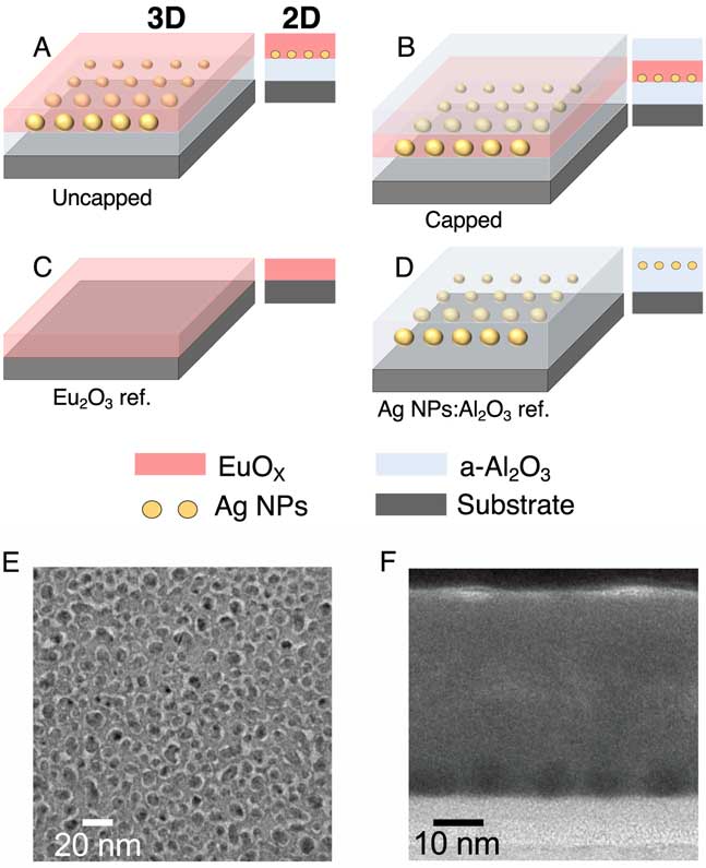
We study the light emission of plasmonic-luminescent hybrid nanostructures consisting of Ag nanoparticles (NPs) embedded in europium oxide (EuOX). The Ag NPs present a bidimensional organization in the nanostructures and they optically behave as oblate spheroids. The photoluminescence (PL) spectral response of the nanostructures evolves from a narrow red emission characteristic of Eu3+ ions in absence of Ag NPs to a broad blue-green emission band associated with Eu2+ ions when the layer of Ag NPs is present. This behavior is not related to a change in the Eu2+/Eu3+ ratio, which is verified by compositional analysis. Instead, a detailed investigation of the PL emission of the nanostructures suggests that the coupling of the Ag NPs to the Eu2+ ions present in the EuOX layer, which manifests itself in an efficient sensitization of these ions, enhances their broad visible emission. In particular, the longitudinal mode of the Ag NPs surface plasmon is considered to be responsible for the efficient energy transfer for the non-normal incidence excitation PL configuration used. Finally, the use of a capping amorphous Al2O3 layer allows improving the robustness of hybrid nanostructures and further enhances their PL emission. These findings provide a new path to actively control the selective excitation of Eu2+ and Eu3+ ions via a controlled coupling with the surface plasmon resonance modes of the Ag NPs and points to these nanostructures as promising building blocks for the development of integrable white light sources.

Vapor-solid growth ZnO:ZrO2 micro and nanocomposites

Ariza, R., Dael, M., Sotillo, B., Urbieta, A., Solis, J., Fernández, P.
Journal of Alloys and Compounds, 877, art. no. 160219

Abstract
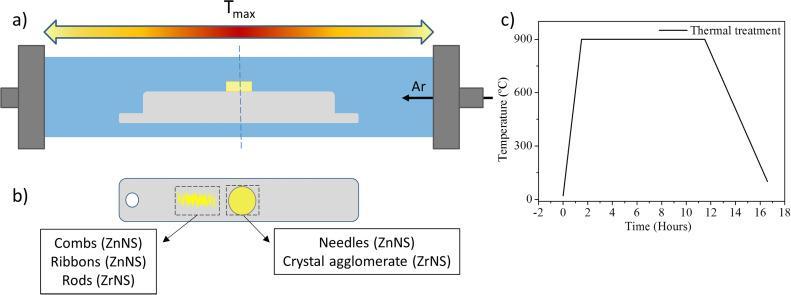
Microstructures of ZnO and ZrO2 and the corresponding composites have been grown by the Vapor-Solid method. A detailed characterization of their structural, compositional and optical properties has been performed. X-ray diffraction (XRD) and Raman spectroscopy measurements, let us identify two main phases, wurtzite ZnO and monoclinic ZrO2, reinforcing the hypothesis of ZnO/ZrO2 composite formation. Scanning Electron Microscopy observations reveal the presence of different morphologies depending on the synthesis conditions. Chemical composition was analyzed by energy dispersive X-ray (EDX) spectroscopy. Luminescence properties were studied by photoluminescence and cathodoluminescence. Our results indicate that doping is occurring in both phases: ZnO is doped with Zr and ZrO2 is doped with Zn. However important differences between Zr rich and Zn rich structures are encountered. While the Zn rich structures are single phase with the characteristic wurtzite crystal structure of ZnO, the Zr rich structures are multiphase with both monoclinic and wurtzite crystal structures present, then leading to formation of the composites with interesting luminescence properties, with intense emissions in the near UV and the visble range, even at room temperature.

Deep Silicon Amorphization Induced by Femtosecond Laser Pulses up to the Mid-Infrared

Garcia-Lechuga, M., Casquero, N., Wang, A., Grojo, D., Siegel, J.
Advanced Optical Materials, 9 (17), art. no. 2100400

Abstract
Direct laser writing of amorphous lines in crystalline silicon has the potential for becoming a flexible alternative to silicon-on-insulator technology for photonic integrated circuits. Yet, the maximum amorphous layer thickness achieved is 60 nm, which is below the requirements for waveguiding at telecom wavelengths. Here, the authors report on different strategies to push the layer thickness beyond today’s limit. To this end, irradiation with femtosecond laser pulses covering an extremely broad wavelength range (515 nm–4 µm) up to the yet unexplored near- and mid-infrared region of silicon transparency is investigated. The results show that much thicker amorphous layers can be obtained upon multipulse irradiation at 3-µm wavelength. The deepest amorphization is achieved in silicon wafers covered with a thick silicon dioxide layer that strongly assists the heat extraction, yielding steep index profiles with a maximum amorphous layer thickness of 128 nm. This superior thickness is compatible with single mode waveguiding for a symmetric waveguide configuration. This study also contributes to a better understanding of the mechanisms involved in laser-induced amorphization.

The effect of annealing temperature on Cu2ZnGeSe4 thin films and solar cells grown on transparent substrates

Ruiz-Perona, A., Sánchez, Y., Guc, M., Kodalle, T., Placidi, M., Merino, J.M., Cabello, F., García-Pardo, M., León, M., Caballero, R.
JPhys Materials, 4 (3), art. no. 034009

Abstract
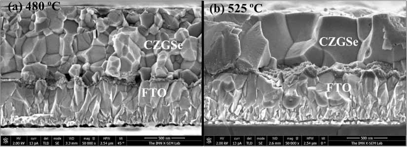
Semi-transparent solar cells are the next step for photovoltaics into our daily life. Over the last years, kesterite-type material has attracted a special attention to be used as an absorber in thin-film solar cells because of its low toxicity and earth abundant constituents. Here, Cu2ZnGeSe4 (CZGSe) thin films are grown by co-evaporation and subsequent annealing at a maximum temperature of 480 °C or 525 °C onto Mo/V2O5/FTO/glass stacks. The goal of this work is to investigate the influence of the annealing temperature on the composition, morphology, vibrational properties, and transmittance of CZGSe layers, the formation of secondary phases, and distribution of elements within the absorber layer as well as on the optoelectronic properties of the corresponding solar cell devices. Raising the annealing temperature to 525 °C leads to a more uniform distribution of Cu, Zn, Ge and Se throughout the absorber layer, a reduction of the presence of the GeSe2 secondary phase, which is mainly detected at 480 °C, a larger grain size and the formation of a thicker MoSe2 layer at the CZGSe/back contact interface. The strategy of increasing the annealing temperature allows for improved J–V characteristics and higher spectral response resulting in an enhanced device performance of 5.3% compared to 4.2% when using 525 °C and 480 °C, respectively. Both absorber layers present an optical band gap energy of 1.47 eV. Furthermore, higher annealing temperature has beneficial effect to the CZGSe-based devices without losses in total transmitted light because of the higher diffuse transmittance. This work shows first promising semi-transparent CZGSe-based solar cells possibly open up new routes of applications.

Competition effects during femtosecond laser induced element redistribution in ba-and la-migration based laser written waveguides

Macias-Montero, M., Moreno-Zárate, P., Muñoz, F., Sotillo, B., Garcia-Pardo, M., Serna, R., Fernandez, P., Solis, J.
Materials, 14 (12), art. no. 3185

Abstract
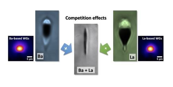
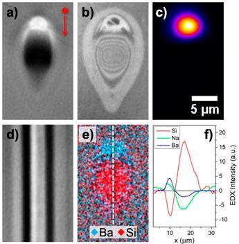
Fs-laser induced element redistribution (FLIER) has been a subject of intensive research in recent years. Its application to various types of glasses has already resulted in the production of efficient optical waveguides, tappers, amplifiers and lasers. Most of the work reported on FLIER-based waveguides refers to structures produced by the cross-migration of alkali (Na, K) and lanthanides (mostly La). The latter elements act as refractive index carrying elements. Herein, we report the production of Ba-based, FLIER-waveguides in phosphate glass with an index contrast > 10−2. Phosphate glasses modified with the same amount of Na2O and K2O, and variable amounts of BaO and/or La2O3 were used to produce the FLIER-waveguides with Ba and or La acting as index carriers. Ba-only modified glasses show a waveguide writing threshold and light guiding performance comparable to that of La-based structures. However, mixed Ba-La glasses show a much higher element migration threshold, and much smaller compositionally modified regions. This behavior is consistent with a competition effect in the cross-migration of both elements (Ba and La) against the alkalis. Such an effect can be applied to inhibit undesired element redistribution effects in fs-laser processing applications in multicomponent glasses

Anisotropic Resistivity Surfaces Produced in ITO Films by Laser-Induced Nanoscale Self-organization

Lopez-Santos, C., Puerto, D., Siegel, J., Macias-Montero, M., Florian, C., Gil-Rostra, J.,López-Flores, V., Borras, A., González-Elipe, A.R., Solis, J.
Advanced Optical Materials, 9 (2), art. no. 2001086

Abstract
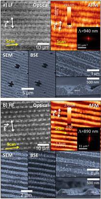
Highly anisotropic resistivity surfaces are produced in indium tin oxide (ITO) films by nanoscale self-organization upon irradiation with a fs-laser beam operating at 1030 nm. Anisotropy is caused by the formation of laser-induced periodic surface structures (LIPSS) extended over cm-sized regions. Two types of optimized structures are observed. At high fluence, nearly complete ablation at the valleys of the LIPSS and strong ablation at their ridges lead to an insulating structure in the direction transverse to the LIPSS and conductive in the longitudinal one. A strong diminution of In content in the remaining material is then observed, leading to a longitudinal resistivity ρL ≈ 1.0 Ω·cm. At a lower fluence, the material at the LIPSS ridges remains essentially unmodified while partial ablation is observed at the valleys. The structures show a longitudinal conductivity two times higher than the transverse one, and a resistivity similar to that of the pristine ITO film (ρ ≈ 5 × 10⁻⁴ Ω·cm). A thorough characterization of these transparent structures is presented and discussed. The compositional changes induced as laser pulses accumulate, condition the LIPSS evolution and thus the result of the structuring process. Strategies to further improve the achieved anisotropic resistivity results are also provided.

Laser‐Empowered Random Metasurfaces for White Light Printed Image Multiplexing

Nathalie Destouches, Nipun Sharma, Marie Vangheluwe, Nicolas Dalloz, Francis Vocanson, Matthieu Bugnet, Mathieu Hébert, Jan Siegel
Advanced Functional Materials (2021).

Abstract

Printed image multiplexing based on the design of metasurfaces has attracted much interest in the past decade. Optical switching between different images displayed directly on the metasurface is performed by altering the parameters of the incident light such as polarization, wavelength, or incidence angle. When using white light, only two-image multiplexing is implemented with polarization switching. Such metasurfaces are made of nanostructures perfectly controlled individually, which provide high-resolution pixels but small images and involve long fabrication processes. Here, it is demonstrated that laser processing of nanocomposites offers a versatile low-cost, high-speed method with large area processing capabilities for controlling the statistical properties of random metasurfaces, allowing up to three-image multiplexing under white light illumination. By independently controlling absorption and interference effects, colors in reflection and transmission can be varied independently yielding two-image multiplexing under white light. Using anisotropy of plasmonic nanoparticles, a third image can be multiplexed and revealed through polarization changes. The design strategy, the fundamental properties, and the versatility of implementation of these laser-empowered random metasurfaces are discussed. The technique, applied on flexible substrate, can find applications in information encryption or functional switchable optical devices, and offers many advantages for visual security and anticounterfeiting.

Femtosecond laser induced thermophoretic writing of waveguides in silicate glass

Manuel Macias-Montero, Francisco Muñoz, Belén Sotillo, Jesús del Hoyo, Rocío Ariza, Paloma Fernandez, Jan Siegel & Javier Solis
Scientific Reports (2021).

Abstract

Here in, the fs-laser induced thermophoretic writing of microstructures in ad-hoc compositionally designed silicate glasses and their application as infrared optical waveguides is reported. The glass modification mechanism mimics the elemental thermal diffusion occurring in basaltic liquids at the Earth’s mantle, but in a much shorter time scale (108 times faster) and over a well-defined micrometric volume. The precise addition of BaO, Na2O and K2O to the silicate glass enables the creation of positive refractive index contrast upon fs-laser irradiation. The influence of the focal volume and the induced temperature gradient is thoroughly analyzed, leading to a variety of structures with refractive index contrasts as high as 2.5 × 10⁻². Two independent methods, namely near field measurements and electronic polarizability analysis, confirm the magnitude of the refractive index on the modified regions. Additionally, the functionality of the microstructures as waveguides is further optimized by lowering their propagation losses, enabling their implementation in a wide range of photonic devices.

Abstract

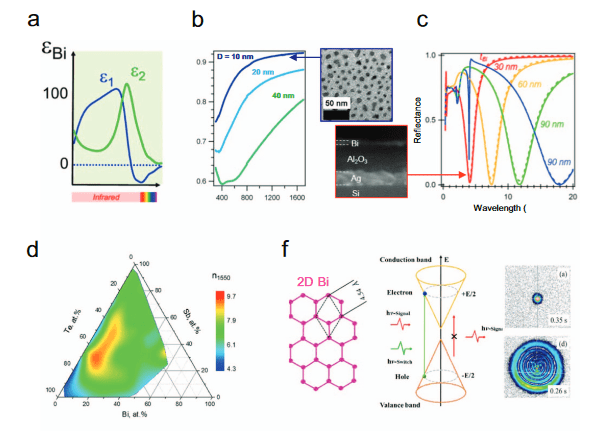
Although plasmonics and high refractive index photonics have experienced very fast growth thanks to classical physics concepts, there is an increasing interest in harnessing quantum physics concepts for further pushing the frontiers of these fields. In this context, this perspective highlights the importance of some quantum nanostructures for building nanomaterials and metamaterials with enhanced plasmonic and high refractive index properties. Two types of nanostructures displaying quantum properties are considered: (a) quantum confined nanostructures consisting of noble metals or standard semiconductors, (b) nanostructures built from alternative materials whose dielectric function and optical properties are driven by (possibly tailored) giant interband electronic transitions. A special emphasis is made on the potential of this latter type of nanostructures for achieving outstanding effects for applications, such as ultrabroadband light harvesting, giant refractive index, coupling between dielectric, low-loss plasmonic and magnetic properties, compositionally or externally tuneable optical response. Possible future developments to the field are discussed.

4 + 6 =

Drop me a line