Grupo de Procesado por Láser del Instituto de Óptica “Daza de Valdés”

Optoplasmonic tuneable response by femtosecond laser irradiation of glass with deep-implanted gold nanoparticles

Irene Solana, María Dolores Ynsa, Fátima Cabello, Fernando Chacon-Sanchez, Jan Siegel, Mario Garcia-Lechuga
Materials Today Nano, 28 (2024) 100526
Abstract
The manipulation of the optical properties of plasmonic nanocomposites is of high interest for the development of advanced optical devices with tailored unique properties. Achieving these objectives requires a combination of synthesis techniques and post-fabrication strategies. Here, we combine the use of two well-established physical strategies: MeV ion implantation and femtosecond laser processing. Firstly, we synthesize Au-doped soda lime glass nanocomposite through ion beam implantation (Au2+ at 1.8 MeV) followed by thermal annealing. This synthesis procedure results in a peculiar optical response based on the combination of Au-nanoparticle plasmonic resonance and a Fabry-Perot interference, caused by the deep implantation (centered at 480 nm). Secondly, this dual response is demonstrated to be highly tuneable by non-resonant femtosecond laser irradiation (800-nm wavelength and 130-fs pulse duration). Depending on the laser fluence, three transformation regimes are distinguished: supressing the interferometric response by spallative ablation, inducing vivid blue colors by surface swelling, and producing red-shifted color changes by multi-shot irradiation at low fluences. The proposed method is very versatile, since it is applicable to any dielectric matrix or implanted element. This work paves the way to a new route for the development of scalable and tuneable nanocomposites with several potential applications in optics.

Optoelectronic properties of GaP:Ti photovoltaic devices

J. Olea, J. Gonzalo, J. Siegel, A.F. Braña, G. Godoy-Pérez, R. Benítez-Fernández, D. Caudevilla, S. Algaidy, F. Pérez-Zenteno, S. Duarte-Cano, A. del Prado, E. García-Hemme, R. García-Hernansanz, D. Pastor, E. San-Andrés, I. Mártil
Materials Today Sustainability Volume 28, December 2024, 101008
Abstract
Supersaturated GaP is of interest for the photovoltaic field since optical transitions at energies below the bandgap (2.26 eV) could enhance the overall device efficiency up to theoretically 60%. We have previously demonstrated that Ti supersaturated GaP can be obtained by means of ion implantation and pulsed-laser melting with high structural quality and measured its below-bandgap photoconductivity. In this work we report the first results of a GaP:Ti based photovoltaic device. We have fabricated and measured photovoltaic devices with a GaP:Ti absorber layer showing enhanced external quantum efficiency at wavelengths above 550 nm. Also, we have measured the absorption coefficient (around 104 cm−1) and refractive index of this absorber layer. Finally, current-voltage curves in darkness were measured and analyzed using a two-diodes model, showing improvable characteristics. Ideas to enhance the properties of the devices are suggested.

Exploring OH incorporation pathways in pulsed laser deposited EuOOH thin films

E. Nieto-Pinero, G. Gorni, A. Caño, A. Mariscal-Jimenez, E. Briand, I. Trimaille, J.-J. Ganem, I. Vickridge, R. Serna, J. Gonzalo
Applied Surface Science, Volume 670, 15 October 2024, 160581
Abstract
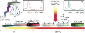
This study sheds light on the formation of EuOOH thin films intended for photonic applications in light emission. To this end, we designed a unique experiment in which we deposited films by pulsed laser deposition from an Eu2O3 target followed by low temperature annealing in an isotopic furnace, which allows selecting atmospheres (18O2 or D218O vapour) containing specific isotopes. Ion beam techniques have been used for the absolute determination of 16O and H content as well as that of the isotopes (18O, D) incorporated in the films upon annealing. A large content of either H2O or hydroxyl (OH−) groups was identified in the as-deposited films by infrared spectroscopy, while the incorporation of 18O or D upon annealing is limited (≤8 % and ≤ 4 %, respectively). Yet, annealing is a critical and necessary step to achieve the right stoichiometry and to induce the formation of hydroxides. Films produced under the optimum deposition pressure range (≤4 × 10⁻⁴ Pa) and annealing atmosphere (D218O) show the EuOOH monoclinic structure, while their photoluminescence response is in excellent agreement with the emission of Eu3+ ions in monoclinic EuOOH.

Tailoring the Lithium Concentration in Thin Lithium Ferrite Films Obtained by Dual Ion Beam Sputtering

Pilar Prieto, Cayetano Hernández Gómez, Sara Román Sánchez, Marina París Ogáyar, Giulio Gorni, José Emilio Prieto, Aida Serrano
Nanomaterials Volume 14, Issue 14July 2024 Article number 1220
Abstract
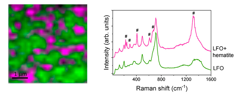
Thin films of lithium spinel ferrite, LiFe5O8, have attracted much scientific attention because of their potential for efficient excitation, the manipulation and propagation of spin currents due to their insulating character, high-saturation magnetization, and Curie temperature, as well as their ultra-low damping value. In addition, LiFe5O8 is currently one of the most interesting materials in terms of developing spintronic devices based on the ionic control of magnetism, for which it is crucial to control the lithium’s atomic content. In this work, we demonstrate that dual ion beam sputtering is a suitable technique to tailor the lithium content of thin films of lithium ferrite (LFO) by using the different energies of the assisting ion beam formed by Ar+ and O2+ ions during the growth process. Without assistance, a disordered rock-salt LFO phase (i.e., LiFeO2) can be identified as the principal phase. Under beam assistance, highly out-of-plane-oriented (111) thin LFO films have been obtained on (0001) Al2O3 substrates with a disordered spinel structure as the main phase and with lithium concentrations higher and lower than the stoichiometric spinel phase, i.e., LiFe5O8. After post-annealing of the films at 1025 K, a highly ordered ferromagnetic spinel LFO phase was found when the lithium concentration was higher than the stoichiometric value. With lower lithium contents, the antiferromagnetic hematite (α-Fe2O3) phase emerged and coexisted in films with the ferromagnetic LixFe6-xO8. These results open up the possibility of controlling the properties of thin lithium ferrite-based films to enable their use in advanced spintronic devices.

Amorphization and Ablation of Crystalline Silicon Using Ultrafast Lasers: Dependencies on the Pulse Duration and Irradiation Wavelength

Mario Garcia-Lechuga, Noemi Casquero, Jan Siegel, Javier Solis, Raphael Clady, Andong Wang, Olivier Utéza and David Grojo
Laser and Photonics Reviews
Abstract
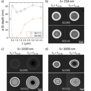
Using lasers to achieve controlled crystallographic phase changes in silicon with high spatial precision promises new manufacturing solutions in semiconductor technologies, including silicon photonics. Recent demonstrations of improved amorphization thicknesses position ultrafast lasers as an optimum tool to meet current challenges. Here, the literature on silicon transformations is reviewed and complemented with new experimental data. This includes amorphization and ablation response as a function of pulse duration (τ = 13.9 to 134 fs at λ = 800 nm) and laser wavelength (λ = 258 to 4000 nm with τ = 200 fs pulses). For pulse duration-dependent studies on Si(111), the amorphization fluence threshold decreases with shorter durations, emphasizing the significance of non-linear absorption in the range of considered conditions. For wavelength-dependent studies, the amorphization threshold increases sharply from λ = 258 to 1030 nm, followed by near-constant behavior up to λ = 3000 nm. Conversely, the ablation threshold fluence increases in these specified ranges. Differences in the obtained amorphization thicknesses on Si(111) and Si(100) are also discussed, identifying an anomalously large fluence range for amorphization at λ = 258 nm. Finally, the question of the lateral resolution, shown as independent of the interaction nonlinearity is addressed.

Building nanoplatelet α-MoO3 films: A high quality crystal anisotropic 2D material for integration

E. Nieto-Pinero, S. Negrete-Aragón, I. Muñoz Ochando, M. Vondráček, B. Galiana, R.J. Pelaéz, B. Maté, S. López-Andrés, R. Serna
Applied Surface Science Volume 6721 Article number 160871
Abstract

The successful development of nanoplatelet α-MoO3 −films with wavelength-dependent in-plane and out-of-plane birefringence both in the visible and in the medium infrared is demonstrated. The films are prepared by a two-step process starting from structurally amorphous and continuous substoichiometric MoO3-X followed by isothermal annealing at low temperature (250 °C) to yield the formation of a dense network of large α-MoO3 2D nanoplatelets lying in-plane with no overlapping. These α-MoO3 crystals form a film with excellent thickness uniformity (20 nm) and are oriented with the [0 1 0] crystallographic direction parallel to the substrate normal. Finally, we report the film anisotropic optical complex refractive index, both parallel and perpendicular to the plane the full spectral range from 0.7 to 5 eV as determined by spectroscopic ellipsometry, and their characteristic in-plane phonon mode in the IR from FTIR measurements. These results show a promising pathway to the creation of highly functional anisotropic α-MoO3 2D films suitable for the development of integrated nanostructured photonic components.

Out-of-plane preferential growth of 2D molybdenum diselenide nanosheets on laser-induced periodic surface structures

A. Fernández García a, R. Ariza b d, J. Solis b, F. Agulló-Rueda c, M. Manso Silvan a, M. Garcia-Lechuga
Applied Surface Science. Volume 669, 22 June 2024, 160567
Abstract
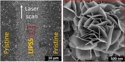
In this study, we explore the morphology and orientation of molybdenum diselenide, a Van der Waals 2D material, through isothermal closed space vapor deposition on both pristine and laser-structured substrates. Laser structuring is conducted on dielectric (sapphire), semiconductor (silicon), and conductive (titanium nitride) substrates using ultrashort laser pulses, resulting in smooth topographic changes such as laser-induced periodic surface structures (LIPSS) or selective ablation. Scanning electron microscopy (SEM) reveals the pivotal role of surface structuring in the growth of out-of-plane MoSe2 nanosheets. This effect is particularly pronounced on monocrystalline substrates like sapphire and silicon, exhibiting in-plane growth on pristine substrates. Additionally, Raman spectroscopy confirms the vertical orientation of flakes on structured substrates and highlights the presence of active edge sites by demonstrating an increased abundance of deposited material. Overall, our findings emphasize the controllability of directing the growth of MoSe2 flakes through appropriate pre-treatment of the substrate, with potential applications in various fields, including Surface-Enhanced Raman Scattering (SERS). Furthermore, the scalability, reproducibility, and applicability to any substrate make ultrashort laser structuration a promising general strategy for orienting 2D materials.

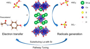
Composition-dependent PMS activation in SrxLa2-xCoO4±δ perovskite-derivatives: From radical to strengthen the electron-transfer pathway

Yu Shen, María J. Martín de Vidales, Giulio Gorni, Maria J. Sampaio, Adrián M.T. Silva, Ana R. Lado Ribeiro, Antonio J. Dos santos-García
Applied Catalysis B: Environmental, 357, art. no. 124291. June 2024
Abstract

Ruddlesden-Popper phases (R-P) with the chemical formula SrxLa2-xCoO4±δ (x=0.6, 0.8, 1.0, 1.2, and 1.5), consisting of alternating layers of perovskite and rock-salt type oxides, were found to be efficient catalysts for peroxymonosulfate (PMS) activation. By modifying the strontium content, it is possible to tune the spin state of cobalt in the material, which in turn affects the PMS activation mechanism. When the rock-salt layer is intercalated in the R-P perovskite structure, as in Sr0.8La1.2CoO4, a non-radical pathway is involved, which exhibits superior performance in PMS activation, as indicated by the higher reaction rate constant (0.70 min−1) compared to LaCoO3 (0.13 min−1) with SO4 generation as the primary mechanism.

This research provides a deeper understanding of how the electronic structure of cobalt in perovskite oxides influences the PMS activation mechanism. Such insights are crucial for the rational design of effective PMS activators for water treatment.

Dynamics of phase transformations in Si and Ge upon strong excitation with UV femtosecond laser pulses

Daniel Puerto, Javier Solis, Jan Siegel
Applied Surface Science, Volume 666, 31 May 2024
Abstract
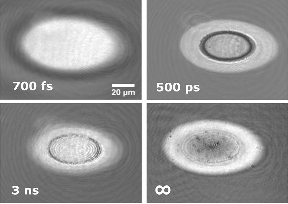
Femtosecond laser processing of semiconductors has evolved into a mature, high-precision fabrication technique, enabling a wide range of applications. While initially most studies have employed pulses at near infrared wavelengths, the interest in using UV laser pulses is constantly increasing due to the different excitation conditions as a consequence of the much shorter optical penetration depth, leading to an improved resolution. In this context, fundamental studies on the temporal dynamics of phase transformations triggered by such pulses are necessary in order to comprehend and eventually control the complex phase transformation pathways. Here, we report a detailed time-resolved study on the phase transformation dynamics of crystalline silicon and germanium upon irradiation with single 400 nm, 100 fs laser pulses in the moderate and high excitation regime. To this end, we have employed fs-resolved optical microscopy with a probe wavelength of 800 nm to study the reflectivity evolution of the irradiated surface over a temporal window ranging from 100 fs up to 20 ns. At moderate excitation fluence, the data reveals the entire sequence of laser-induced processes, starting from the generation of a free-electron plasma, non-thermal melting, ablation onset and expansion of a semi-transparent ablation layer with sharp interfaces. At excitation with peak fluences more than 30 times the ablation threshold, an anomalous transient high-reflectivity state is observed, which might be indicative of a recoil pressure-induced liquid–liquid phase transition. Moreover, 70 nm-thick amorphous surface layers are formed in both materials after irradiation at moderate fluences. Overall, our results provide relevant information on both, transformation dynamics and final state of both materials for fs-pulse excitation in the near-UV wavelength range.

Optical, Electrical, and Optoelectronic Characterization of Ti-Supersaturated Gallium Arsenide

Sari Algaidy, Daniel Caudevilla, Guillermo Godoy-Pérez, Rafael Benítez-Fernández, Francisco Pérez-Zenteno, Sebastián Duarte-Cano, Rodrigo García-Hernansanz, Enrique San Andrés, Eric García-Hemme, Javier Olea, Jan Siegel, José Gonzalo, David Pastor, Álvaro del Prado
Physica status solidi (a). 26 April 2024
Abstract
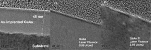
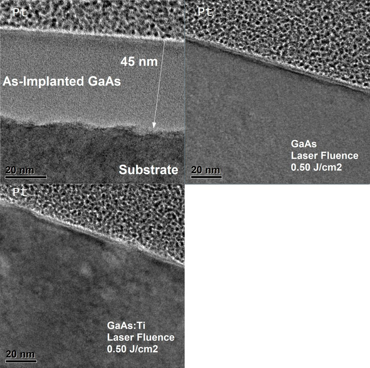
Herein, a detailed investigation on the properties of supersaturated gallium arsenide (GaAs) using Ti+ implantation followed by nanosecond pulsed laser melting (PLM) is presented. The supersaturated samples are analyzed by means of electrical, optical, and optoelectronic characterization. The sheet resistance results obtained using van der Pauw configuration measurements do not show activation of the implanted Ti+ in semi-insulating GaAs after PLM. Absorptance measurements show a sub-bandgap absorption (up to 6.5% for λ = 1000 nm) of the supersaturated GaAs:Ti and the just PLM-processed GaAs, with the same laser melting fluence used (0.50 J/cm−2). The origin of this sub-bandgap absorption is analyzed. Optoelectronic measurements show a similar sub-bandgap photo-response related to the absorption analyzed. The photo-response measured below the bandgap originates from point defects introduced by the PLM process.

Unveiling the non-innocence of vanadium dopant in TiO2 nanocrystals for advanced energy storage and smart windows

Miguel García-Tecedor, Ignacio J Villar-García, Giulio Gorni, Marta Liras, Víctor de la Peña O´Shea and Mariam Barawi
JPhys Energy 6 025024
Abstract
Vanadium doped TiO2 NCs stand out as a promising candidate for energy storage applications due to its high electrical conductivity and redox properties. However, the thermodynamical behavior of the material under working conditions has not been explored and the reasons for its superior performance remain unlocked. This study explores the use of a combination of advanced in situ spectroscopy techniques, including x-ray absorption spectroscopy (XAS), spectro-electrochemistry (SEC), and electrochemical impedance spectroscopy (EIS) to provide unprecedented insights into the intricate electrochemical reaction mechanisms within these nanocrystals. Density functional theory calculations and EIS reveal the active role of substitutional V ions in the TiO2 anatase network as electron donors, enhancing surface charge and carrier density and improving pseudocapacitive properties. Cyclic voltammetry and in situ SEC reveal that V-doped TiO2 NCs exhibit significantly improved charge storage capacities, particularly in the pseudo-capacitance storage mechanism. In situ SEC and XAS analyses indicate that a more effective reduction of Ti4+ ions occurs during the electrochemical process in doped NCs, leading to higher charge capacitance and faster processes. Furthermore, in situ XAS measurements of the V K-edge revealed that the vanadium ions, beyond improving the redox behavior of the host, also actively participate in the reduction process. The significant changes in the V K-edge XANES and extended x-ray absorption fine structure spectra observed under reduction conditions can be ascribed to a change in the structure and oxidation state of the vanadium ions during the electrochemical reaction.

Semitransparent Wide Bandgap Cu2ZnGe(S,Se)4 Thin-Film Solar Cells: Role of the Sulfurization Process

Andrea Ruiz-Perona, David Palma-Lafuente, Yudania Sánchez, Maxim Guc, Tim Kodalle, Mohamed Ould Salem, Marcel Placidi, Rosalia Serna, Alejandro Pérez-Rodríguez, José Manuel Merino, Raquel Caballero
Solar RRL, February 2024, Volume 8, Issue 4, Article number 2300947
Abstract
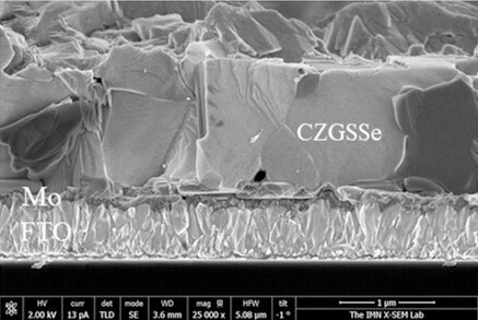
Semitransparent solar cells are very attractive due to the increasing integration in daily life. Kesterite-type based thin-film solar cells stand out because of its environmentally benign composition and outstanding stability. Herein, the influence of the back contact (Mo/V2O5/FTO or Mo/FTO) and thickness of Cu2ZnGe(S,Se)4 (CZGSSe) absorber layer, grown by sulfurization of coevaporated CZGSe, is investigated. To increase the transparency, thinner absorber layers with higher bandgap energy are produced. A double sulfur gradient through the CZGSSe layer with a considerable S content near the back contact and the formation of Mo(S,Se)2 phase at the back interface is detected for an absorber of only 400 nm thickness. Efficiencies of 3.1% and 2.7% are achieved for 1.2 μm CZGSSe-based devices with Eg of 1.73 and 1.86 eV, respectively, while enabling transmittance values higher than 20% in the near-infrared (NIR). The highest transmittance, 40% in the NIR, is achieved for the 400 nm CZGSSe-based solar cells with Eg of 2.1 eV; however, a significant reduction of these devices’ performance is obtained due to the presence of ZnS secondary phase and a different back-contact interface formation. This work presents the first promising semitransparent CZGSSe solar cells, opening new paths of applications.

Versatile femtosecond laser interference patterning applied to high-precision nanostructuring of silicon

Irene Solana, Fernando Chacon-Sanchez, Mario Garcia-Lechuga, Jan Siegel
Optics & Laser Technology. Volume 179, December 2024, 111360
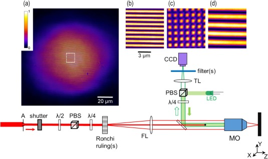
Abstract
In this work we present a route for fabricating WTe2 thin-films together with femtosecond laser post processing, enabling to finely control the conductivity. First, we produce amorphous films of WO3 on Si by spin-coating a sol-gel precursor followed by a consolidating annealing and a reduction process in partial H2 atmosphere, leading to porous metallic tungsten cluster layers. To achieve WTe2, the films were exposed to the chalcogen vapours by isothermal closed space vapor transport. The formation of a tungsten ditelluride film composed of piled crystals could be confirmed and a gradient of surface rich Te identified through hard X-ray photoelectron spectroscopy. Finally, it is demonstrated that resistivity can be changed from 0.2 mΩ.m to 1 mΩ.m, while keeping the material characteristics. An anisotropic conductivity can be induced by direct selective thinning with fs laser writing (350 fs pulse duration, 515 nm laser wavelength) of 1D stripes. The obtained results, demonstrate that laser processing is a promising thin-film post-processing technique that can be applied to 2D transition metal dichalcogenide thin films.

Femtosecond laser thinning for resistivity control of tungsten ditelluride thin-films synthesized from sol-gel deposited tungsten oxide

A. Fernández García a, M. Garcia-Lechuga b, F. Agulló Rueda c, J. Rubio Zuazo c d, M. Manso Silvan
Surfaces and Interfaces. Volume 44, January 2024, 103668
Abstract
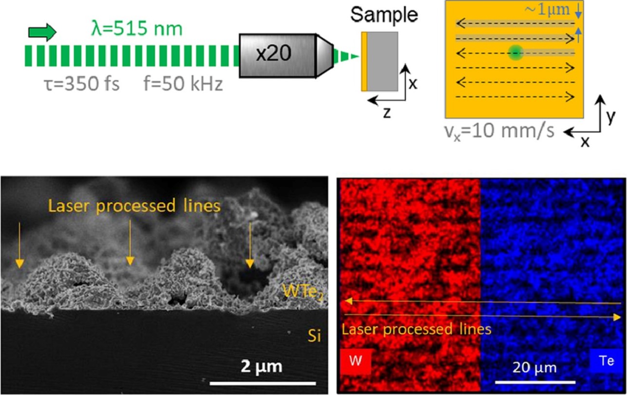
In this work we present a route for fabricating WTe2 thin-films together with femtosecond laser post processing, enabling to finely control the conductivity. First, we produce amorphous films of WO3 on Si by spin-coating a sol-gel precursor followed by a consolidating annealing and a reduction process in partial H2 atmosphere, leading to porous metallic tungsten cluster layers. To achieve WTe2, the films were exposed to the chalcogen vapours by isothermal closed space vapor transport. The formation of a tungsten ditelluride film composed of piled crystals could be confirmed and a gradient of surface rich Te identified through hard X-ray photoelectron spectroscopy. Finally, it is demonstrated that resistivity can be changed from 0.2 mΩ.m to 1 mΩ.m, while keeping the material characteristics. An anisotropic conductivity can be induced by direct selective thinning with fs laser writing (350 fs pulse duration, 515 nm laser wavelength) of 1D stripes. The obtained results, demonstrate that laser processing is a promising thin-film post-processing technique that can be applied to 2D transition metal dichalcogenide thin films.

Building Conventional Metasurfaces with Unconventional Interband Plasmonics: A Versatile Route for Sustainable Structural Color Generation Based on Bismuth

Fernando Chacon-Sanchez, Carlota Ruiz de Galarreta, Eva Nieto-Pinero, Marina Garcia-Pardo, Elisa Garcia-Tabares, Nicolas Ramos, Miguel Castillo, Martin Lopez-Garcia, Jan Siegel, Johann Toudert, C. David Wright, Rosalia Serna
Advanced Optical Materials, Volume12, Issue10. April 4, 2024
Abstract
Plasmonic metasurfaces for structural color generation are typically built using the archetypal noble metals, gold, and silver. These possess plasmonic properties in the visible spectrum due to their inherent high free carrier densities. However, they are much more expensive compared to many other metals and exhibit several nanofabrication issues such as bad surface adhesion or thermally activated inter-diffusion. In this work, it is shown that interband plasmonic materials –whose optical properties are driven by interband transitions instead of free carriers— are appealing candidates for the fabrication of sustainable and cost-efficient metasurfaces for structural coloring. By using bismuth, an environment-friendly interband plasmonic material cheaper than gold and silver, nanodisks gap-plasmon metasurfaces and planar Fabry-Perot cavities are modeled and fabricated, which both successfully enable pure colors that can be robustly tailored upon suitable design. By direct experimental comparison between both types of design in terms of color efficiency, fabrication complexity, and angular robustness; how bismuth-based gap surface plasmon metasurfaces can be excellent candidates for color microprinting is shown, whereas nanolayered Bi Fabry-Pérot cavities are ideal for macroscopic color coatings due to their ease of fabrication and implementation.

Optical, Electrical, and Optoelectronic Characterization of Ti-Supersaturated Gallium Arsenide

Sari Algaidy, Daniel Caudevilla, Guillermo Godoy-Pérez, Rafael Benítez-Fernández, Francisco Pérez-Zenteno, Sebastián Duarte-Cano, Rodrigo García-Hernansanz, Enrique San Andrés, Eric García-Hemme, Javier Olea, Jan Siegel, José Gonzalo, David Pastor, Álvaro del Prado
Physica Status Solidi (A) Applications and Materials Science. April 26, 2024
Abstract
Herein, a detailed investigation on the properties of supersaturated gallium arsenide (GaAs) using Ti+ implantation followed by nanosecond pulsed laser melting (PLM) is presented. The supersaturated samples are analyzed by means of electrical, optical, and optoelectronic characterization. The sheet resistance results obtained using van der Pauw configuration measurements do not show activation of the implanted Ti+ in semi-insulating GaAs after PLM. Absorptance measurements show a sub-bandgap absorption (up to 6.5% for λ = 1000 nm) of the supersaturated GaAs:Ti and the just PLM-processed GaAs, with the same laser melting fluence used (0.50 J/cm−2). The origin of this sub-bandgap absorption is analyzed. Optoelectronic measurements show a similar sub-bandgap photo-response related to the absorption analyzed. The photo-response measured below the bandgap originates from point defects introduced by the PLM process.

7 + 10 =

Drop me a line