Grupo de Procesado por Láser del Instituto de Óptica “Daza de Valdés”

Influence of Heat Accumulation on Morphology Debris Deposition and Wetting of LIPSS on Steel upon High Repetition Rate Femtosecond Pulses Irradiation

Camilo Florian, Yasser Fuentes-Edfuf, Evangelos Skoulas, Emmanuel Stratakis, Santiago Sanchez-Cortes, Javier Solis, Jan Siegel
Materials, Volume 15
Abstract
The fabrication of laser-induced periodic surface structures (LIPSS) over extended areas at high processing speeds requires the use of high repetition rate femtosecond lasers. It is known that industrially relevant materials such as steel experience heat accumulation when irradiated at repetition rates above some hundreds of kHz, and significant debris redeposition can take place. However, there are few studies on how the laser repetition rate influences both the debris deposition and the final LIPSS morphology. In this work, we present a study of fs laser-induced fabrication of low spatial frequency LIPSS (LSFL), with pulse repetition rates ranging from 10 kHz to 2 MHz on commercially available steel. The morphology of the laser-structured areas as well as the redeposited debris was characterized by scanning electron microscopy (SEM) and µ-Raman spectroscopy. To identify repetition rate ranges where heat accumulation is present during the irradiations, we developed a simple heat accumulation model that solves the heat equation in 1 dimension implementing a Forward differencing in Time and Central differencing in Space (FTCS) scheme. Contact angle measurements with water demonstrated the influence of heat accumulation and debris on the functional wetting behavior. The findings are directly relevant for the processing of metals using high repetition rate femtosecond lasers, enabling the identification of optimum conditions in terms of desired morphology, functionality, and throughput.

Ultrafast Electron Dynamics and Optical Interference Tomography of Laser Excited Steel

Yasser Fuentes-Edfuf, Mario Garcia-Lechuga, Javier Solis, Jan Siegel
Laser & Photonics Reviews, Volume 16

Abstract
Femtosecond laser machining of materials has transformed into a mature high-precision technology, giving access to a wide range of applications. Yet, for a complete exploitation of its full potential, a detailed knowledge of the complex laser–matter interaction processes is required. For the case of the application-relevant material steel, a complete study of the electron dynamics and material transformation upon single laser pulse irradiation (800 nm, 120 fs) is reported. Detailed analysis of the obtained time- and fluence-dependent reflectivity map reveals that ultrafast electron heating during the pulse is directly followed by energy transfer to the lattice within a few picoseconds, reaching fluence-dependent peak temperatures from below melting threshold to above the boiling point. Moreover, an innovative approach to obtain the ultrafast-evolving 3D structure of a femtosecond laser excited material is reported, unraveling the dynamics of complex processes as melting, ablation, and solidification. Combined with modeling, the evolving optical properties, multilayer structure, and expansion velocities can be precisely determined. The information obtained from this study will contribute to further increase the achievable precision and wealth of structures that can be produced by designing efficient pulsed energy deposition schemes for selective re-excitation of the material.

Spectroscopic ellipsometry study of Cu2Zn(GexSi1-x)Se4 bulk poly-crystals

ElenaHajdeu-Chicarosh, Sergiu Levcenko, Rosalia Serna, Ivan V. Bodnar, Ivan A. Victorov, Oxana Iaseniuc, Raquel Caballero, José Manuel Merino, Ernest Arushanov, Máximo León
Solid State Sciences, Volume 132

Abstract
The present study addresses to the synthesis and determination of the dielectric function of Cu2Zn(GexSi1-x)Se4 solid solutions with x = 0.4 and 0.8 over the range 1–4.5 eV by spectroscopic ellipsometry analysis, with the aim to achieve a suitable band gap tuning. The dielectric function of the samples is determined using the Adachi model. From the analysis the lowest E0 transition and high energy E1A and E1B transitions are identified. It is found that the band gap varies nonlinearly on composition in the Cu2Zn(GexSi1-x)Se4 alloys and band gap values as large as 1.87 eV are obtained. These results are essential for the design of efficient tailored photovoltaic solar cells and show the high potential of the kesterite compounds for the development of low-cost sustainable future solar cells.

Propagation dynamics of the solid-liquid interface in Ge upon ns and fs laser irradiation

Noemi Casquero, Carlota Ruiz de Galarreta, Yasser Fuentes-Edfuf, Javier Solis, C. David Wright, and Jan Siegel
J. Phys. D: Appl. Phys. 55, 365104 (2022)
Abstract
Monitoring the laser-induced melting and solidification dynamics of Ge upon laser irradiation is an enormous challenge due to the short penetration depth of its liquid phase. In this work, real-time pump-probe experiments in combination with finite element calculations have been employed to investigate the melting and solidification dynamics of germanium upon ns and fs laser pulse irradiation (λ = 800 nm). Excellent agreement between experiments and simulations allowed us to indirectly determine additional time- and depth-dependent information about the transformation dynamics of germanium, including the thickness evolution of the molten layer, as well as its melting and solidification velocities for the two pulse durations for different fluences. Our results reveal considerable differences in the maximum thickness of the molten Ge superficial layers at sub-ablative fluences for ns and fs pulses, respectively. Maximum melt-in velocities of 39 m s−1 were obtained for ns pulses at high fluences, compared to non-thermal melting of a thin layer within 300 fs for fs pulses already at moderate fluences. Maximum solidification velocities were found to be 16 m s−1 for ns pulses, and up to 55 m s−1 for fs pulses. Weak signs of amorphization were observed for fs excitation, suggesting that the lower limit of solidification velocities for a complete amorphization is above 55 m s−1. In addition, we show high precision measurements of the melt-in velocities over the first 20 nm by means of fs microscopy with sub-ps temporal resolution. Here, differences of the melt-in process of several orders of magnitude were observed, ranging from virtually instantaneous melting within less than 2 ps even for a moderate peak fluence up to 200 ps for fluences close to the melting threshold.

Pulsed laser deposition and structural evolution of BaF2 nanolayers in Eu-doped BaF2/Al2O3 layered optical nanocomposite thin films

Yu Jin, Charles W.Bond, Pilar Gomez-Rodrigue, Eva Nieto-Pinero, Russell L. Leonard, David J. Gosztola, Jacqueline A. Johnson, Jose Gonzalo, Rosalia Serna, Amanda K. Petford-Long
Thin Solid Films, Volume 754

Abstract
We have developed a pulsed laser deposition (PLD) geometry for the growth of uniform BaF2 nanoscale thin films, through control of the deposition conditions. Our goal is to use the BaF2 layers with controllable structure as component layers in layered optical nanocomposites. The structure of the BaF2 nanolayer evolves as a function of the layer thickness: BaF2 grows via a layer-by-layer growth mode on Al2O3; the layers are amorphous for a thickness < 3 nm, and then become nanocrystalline as the layer thickness increases. The BaF2 nanocrystals have an FCC crystal structure with a weak <111> texture that becomes stronger for thicker films. We then demonstrate that our BaF2 films can be introduced into layered Al2O3/BaF2/EuOx nanocomposite films, which allows for control of the relative position of the Eu ions and the BaF2 layer. Cross-section samples of the multilayered films show interfacial intermixing between the layers, which is related to implantation during the PLD process. This intermixing enables the incorporation of Eu ions into BaF2 layers and form a thin Eu-doped BaF2 nanolayer at the interface. The layered nanocomposite films show photoluminescence (PL) emission from Eu3+ ions, and the PL intensity changes can be correlated with the crystallinity and crystal size changes in the BaF2 layer. Our results provide guidance for achieving thin film nanocomposite materials with controllable structure and photoluminescence behavior for light emitting diodes, photovoltaics and other optical applications.
Gra´fica que muestra la respuesta óptica de las multicapas

Mechanisms driving self-organization phenomena in random plasmonic metasurfaces under multipulse femtosecond laser exposure: A multitime scale study

Balint Eles, Paul Rouquette, Jan Siegel, Claude Amra, Julien Lumeau, Antonin Moreau, Christophe Hubert, Myriam Zerrad and Nathalie Destouches
Nanophotonics, Volume 11 Issue 10

Abstract

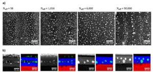
Laser-induced transformations of plasmonic metasurfaces pave the way for controlling their anisotropic optical response with a micrometric resolution over large surfaces. Understanding the transient state of matter is crucial to optimize laser processing and reach specific optical properties. This article proposes an experimental and numerical study to follow and explain the diverse irreversible transformations encountered by a random plasmonic metasurface submitted to multiple femtosecond laser pulses at a high repetition rate. A pump-probe spectroscopic imaging setup records pulse after pulse, and with a nanosecond time resolution, the polarized transmission spectra of the plasmonic metasurface, submitted to 50,000 ultrashort laser pulses at 75 kHz. The measurements reveal different regimes, occurring in different ranges of accumulated pulse numbers, where successive self-organized embedded periodic nanostructures with very different periods are observed by post-mortem electron microscopy characterizations. Analyses are carried out; thanks to laser-induced temperature rise simulations and calculations of the mode effective indices that can be guided in the structure. The overall study provides a detailed insight into successive mechanisms leading to shape transformation and self-organization in the system, their respective predominance as a function of the laser-induced temperature relative to the melting temperature of metallic nanoparticles and their kinetics. The article also demonstrates the dependence of the self-organized period on the guided-mode effective index, which approaches a resonance due to system transformation. Such anisotropic plasmonic metasurfaces have a great potential for security printing or data storage, and better understanding their formation opens the way to smart optimization of their properties.

Gra´fica que muestra la respuesta óptica de las multicapas

Enhanced Light Absorption in All‐Polymer Biomimetic Photonic Structures by Near‐Zero‐Index Organic Matter

Miguel A. Castillo, C. Estévez-Varela, William P. Wardley, R. Serna, I. Pastoriza-Santos, S. Núñez-Sánchez, Martin Lopez-Garcia
Advanced Functional Materials, art. no. 2113039

Abstract

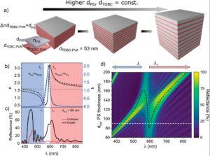
Natural photosynthetic photonic nanostructures can show sophisticated light–matter interactions including enhanced light absorption by slow light even for highly pigmented systems. Beyond fundamental biology aspects, these natural nanostructures are very attractive as blueprints for advanced photonic devices. But the soft-matter biomimetic implementations of such nanostructures is challenging due to the low refractive index contrast of most organic photonic structures. Excitonic organic materials with near-zero index (NZI) optical properties allow overcoming these bottlenecks. Here, it is demonstrated that the combination of NZI thin films with photonic multilayers like the ones found in nature enables broadband tunable strong reflectance as well as slow light absorption enhancement and tailored photoluminescence properties in the full VIS spectrum. Moreover, it is shown that this complex optical response is tunable, paving the way toward the development of active devices based on all-polymer and near-zero index materials photonic structures.

Multiscale ultrafast laser texturing of marble for reduced surface wetting

Ariza, R., Alvarez-Alegria, M., Costas, G., Tribaldo, L., R. Gonzalez-Elipe, A., Siegel, J., Solis, J.
Applied Surface Science, 577, art. no. 151850

Abstract

The modification of the wetting properties of marble surfaces upon multi-scale texturing induced by ultrafast laser processing (340 fs pulse duration, 1030 nm wavelength) has been investigated with the aim of evaluating its potential for surface protection. The contact angle (CA) of a water drop placed on the surface was used to assess the wettability of the processed areas. Although the surfaces are initially hydrophilic upon laser treatment, after a few days they develop a strong hydrophobic behavior. Marble surfaces have been irradiated with different scan line separations to elucidate the relative roles of multi-scale roughness (nano- and micro-texture) and chemical changes at the surface. The time evolution of the contact angle has been then monitored up to 11 months after treatment. A short and a long-term evolution, associated to the combined effect of multi-scale roughness and the attachment of chemical species at the surface over the time, have been observed. XPS and ATR measurements are consistent with the progressive hydroxylation of the laser treated surfaces although the additional contribution of hydrocarbon adsorbates to the wettability evolution cannot be ruled-out. The robustness of the results has been tested by CA measurements after cleaning in different conditions with very positive results.

Nanosecond Laser Switching of Phase-Change Random Metasurfaces with Tunable ON-State

Alvarez-Alegria, M., Siegel, J., Garcia-Pardo, M., Cabello, F., Toudert, J., Haro-Poniatowski, E., Serna, R.
Advanced Optical Materials, 10 (3), art. no. 2101405,

Abstract
Random metasurfaces based on disordered phase-change nanostructures with broadband ultraviolet–visible plasmonic properties are fantastic platforms for the development of active photonic components due to their versatility. Here optical ON–OFF switching upon nanosecond laser irradiation of Bi-based random metasurfaces is demonstrated profiting from the solid–liquid phase transition of the Bi nanostructures. The fast switching time is revealed by using single-pulse real-time reflectivity measurements with sub-nanosecond temporal resolution. A sudden reflectivity decrease is observed upon laser excitation, triggered by heating and melting of the embedded Bi nanostructures of the metasurface. This transient state of low reflectivity remains constant until the Bi solidifies upon cooling, recovering the initial reflectivity level, and showing full reversibility of the process. The duration of this ON-state, defined by characteristic low reflectivity values, can be tuned from 10 to >700 ns by adjusting the nanostructure components of the metasurface and laser fluence. Furthermore, it is demonstrated that this ON–OFF switch process is repeatable for more than 100 000 times without observable degradation of the metasurface. These results pave the way for the development of a new generation of fast, robust, and integrable nanophotonic switching devices.

Single-Step Fabrication of High-Performance Extraordinary Transmission Plasmonic Metasurfaces Employing Ultrafast Lasers

Ruiz de Galarreta, C., Casquero, N., Humphreys, E., Bertolotti, J., Solis, J., Wright, C.D., Siegel, J.
ACS Applied Materials and Interfaces, 14 (2), pp. 3446-3454

Abstract
Plasmonic metasurfaces based on the extraordinary optical transmission (EOT) effect can be designed to efficiently transmit specific spectral bands from the visible to the far-infrared regimes, offering numerous applications in important technological fields such as compact multispectral imaging, biological and chemical sensing, or color displays. However, due to their subwavelength nature, EOT metasurfaces are nowadays fabricated with nano- and micro-lithographic techniques, requiring many processing steps and carrying out in expensive cleanroom environments. In this work, we propose and experimentally demonstrate a novel, single-step process for the rapid fabrication of high-performance mid- and long-wave infrared EOT metasurfaces employing ultrafast direct laser writing. Microhole arrays composing extraordinary transmission metasurfaces were fabricated over an area of 4 mm2 in timescales of units of minutes, employing single pulse ablation of 40 nm thick Au films on dielectric substrates mounted on a high-precision motorized stage. We show how by carefully characterizing the influence of only three key experimental parameters on the processed micro-morphologies (namely, laser pulse energy, scan velocity, and beam shaping slit), we can have on-demand control of the optical characteristics of the extraordinary transmission effect in terms of transmission wavelength, quality factor, and polarization sensitivity of the resonances. To illustrate this concept, a set of EOT metasurfaces having different performances and operating in different spectral regimes has been successfully designed, fabricated, and tested. Comparison between transmittance measurements and numerical simulations has revealed that all the fabricated devices behave as expected, thus demonstrating the high performance, flexibility, and reliability of the proposed fabrication method. We believe that our findings provide the pillars for mass production of EOT metasurfaces with on-demand optical properties and create new research trends toward single-step laser fabrication of metasurfaces with alternative geometries and/or functionalities.

Transparent high conductive Titanium oxynitride nanofilms obtained by nucleation control for sustainable optolectronics

E.Enríqueza, A.Mariscal, R.Serna, J.F.Fernández
Applied Surface Science Volume 574, 1 February 2022

Abstract

Transparent conducting thin films have attracted a lot of interest in last decades because they have become essential electrodes for optoelectronics applications. Indium tin oxide (ITO) is the transparent conductor par excellence with 80% transmittance in the visible range and a resistivity of 10−4 Ω·cm. Unfortunately, ITO is toxic, brittle and very expensive due to the Indium scarcity in the earth’s crust. For this reason, sustainable alternatives are being sought. Titanium oxynitrides are a very interesting alternative, titanium is abundant and its oxynitrides show remarkable mechanical, electrical and optical properties that can be tailored by modifying the N/O ratio. However, achieving the balance between transparency and conductivity to design a suitable electrode is a challenging milestone. In this work we prepared high quality TiON nanofilms by PLD (pulsed laser deposition) in vacuum, tuning the transparency and conducting properties by varying the deposition laser energy to control the N/O ratio. The absence of gases flux achieves defect-free films with transparency up to 50% and similar conductivity to ITO (1.8·102 S/cm). These results open a new line of research for the development of sustainable transparent conducting electrodes based on dense and planar TION films, very useful for electronic and optical devices, solar cells or photonics.

13 + 7 =

Drop me a line